

Molecular beam epitaxial growth of III-V semiconductor ... - KOBRA
Molecular beam epitaxial growth of III-V semiconductor ... - KOBRA
Molecular beam epitaxial growth of III-V semiconductor ... - KOBRA

Create successful ePaper yourself
Turn your PDF publications into a flip-book with our unique Google optimized e-Paper software.
Experimental Growth and Characterization Techniques<br />
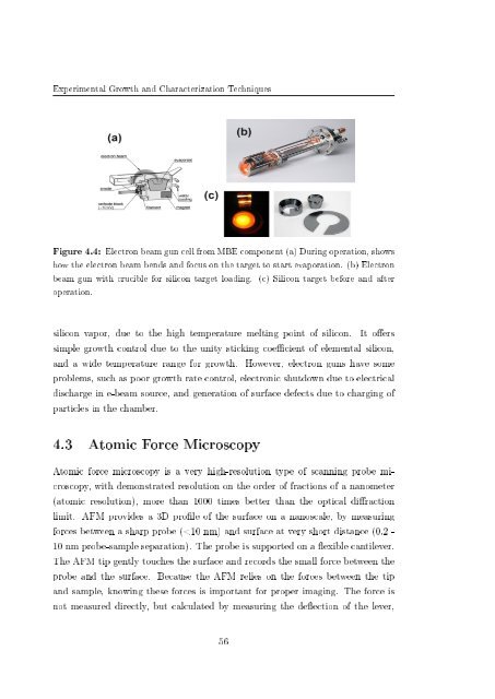
Figure 4.4: Electron <strong>beam</strong> gun cell from MBE component (a) During operation, shows<br />
how the electron <strong>beam</strong> bends and focus on the target to start evaporation. (b) Electron<br />
<strong>beam</strong> gun with crucible for silicon target loading. (c) Silicon target before and after<br />
operation.<br />
silicon vapor, due to the high temperature melting point <strong>of</strong> silicon. It oers<br />
simple <strong>growth</strong> control due to the unity sticking coecient <strong>of</strong> elemental silicon,<br />
and a wide temperature range for <strong>growth</strong>. However, electron guns have some<br />
problems, such as poor <strong>growth</strong> rate control, electronic shutdown due to electrical<br />
discharge in e-<strong>beam</strong> source, and generation <strong>of</strong> surface defects due to charging <strong>of</strong><br />
particles in the chamber.<br />
4.3 Atomic Force Microscopy<br />
Atomic force microscopy is a very high-resolution type <strong>of</strong> scanning probe microscopy,<br />
with demonstrated resolution on the order <strong>of</strong> fractions <strong>of</strong> a nanometer<br />
(atomic resolution), more than 1000 times better than the optical diraction<br />
limit. AFM provides a 3D prole <strong>of</strong> the surface on a nanoscale, by measuring<br />
forces between a sharp probe (


