- Page 1:
Molecular Beam Epitaxial Growth of
- Page 4 and 5:
Gutachter (Supervisors): 1. Prof. D
- Page 6 and 7:
patterns indicating a 2D smooth sur
- Page 8 and 9:
(MEE = migration enhance epitaxy) u
- Page 10 and 11:
viii
- Page 12 and 13:
CONTENTS 3.4.4 Planar Defects Assoc
- Page 14 and 15:
CONTENTS xii
- Page 16 and 17:
Introduction thesis a detailed stud
- Page 18 and 19:
Introduction 1.1.2 Thesis Approach
- Page 20 and 21:
Introduction 1.2 Thesis Outline The
- Page 22 and 23:
Theoretical Background of Semicondu
- Page 24 and 25:
Theoretical Background of Semicondu
- Page 26 and 27:
Theoretical Background of Semicondu
- Page 28 and 29:
Theoretical Background of Semicondu
- Page 30 and 31:
Theoretical Background of Semicondu
- Page 32 and 33:
Theoretical Background of Semicondu
- Page 34 and 35:
Theoretical Background of Semicondu
- Page 36 and 37:
Heteroepitaxial Growth of III-V Sem
- Page 38 and 39:
Heteroepitaxial Growth of III-V Sem
- Page 40 and 41:
Heteroepitaxial Growth of III-V Sem
- Page 42 and 43:
Heteroepitaxial Growth of III-V Sem
- Page 44 and 45:
Heteroepitaxial Growth of III-V Sem
- Page 46 and 47:
Heteroepitaxial Growth of III-V Sem
- Page 48 and 49:
Heteroepitaxial Growth of III-V Sem
- Page 50 and 51:
Heteroepitaxial Growth of III-V Sem
- Page 52 and 53:
Heteroepitaxial Growth of III-V Sem
- Page 54 and 55:
Heteroepitaxial Growth of III-V Sem
- Page 56 and 57:
Heteroepitaxial Growth of III-V Sem
- Page 58 and 59:
Heteroepitaxial Growth of III-V Sem
- Page 60 and 61:
Heteroepitaxial Growth of III-V Sem
- Page 62 and 63:
Heteroepitaxial Growth of III-V Sem
- Page 64 and 65:
Experimental Growth and Characteriz
- Page 66 and 67:
Experimental Growth and Characteriz
- Page 68 and 69:
Experimental Growth and Characteriz
- Page 70 and 71:
Experimental Growth and Characteriz
- Page 72 and 73:
Experimental Growth and Characteriz
- Page 74 and 75:
Experimental Growth and Characteriz
- Page 76 and 77:
Experimental Growth and Characteriz
- Page 78 and 79:
MBE Growth of Self-Assembled InAs a
- Page 80 and 81:
MBE Growth of Self-Assembled InAs a
- Page 82 and 83:
MBE Growth of Self-Assembled InAs a
- Page 84 and 85:
MBE Growth of Self-Assembled InAs a
- Page 86 and 87:
MBE Growth of Self-Assembled InAs a
- Page 88 and 89:
MBE Growth of Self-Assembled InAs a
- Page 90 and 91: MBE Growth of Self-Assembled InAs a
- Page 92 and 93: MBE Growth of Self-Assembled InAs a
- Page 94 and 95: MBE Growth of Self-Assembled InAs a
- Page 96 and 97: MBE Growth of Self-Assembled InAs a
- Page 98 and 99: MBE Growth of Self-Assembled InAs a
- Page 100 and 101: MBE Growth of Self-Assembled InAs a
- Page 102 and 103: MBE Growth of Self-Assembled InAs a
- Page 104 and 105: MBE Growth of Self-Assembled InAs a
- Page 106 and 107: MBE Growth of Self-Assembled InAs a
- Page 108 and 109: MBE Growth of Self-Assembled InAs a
- Page 110 and 111: MBE Growth of Self-Assembled InAs a
- Page 112 and 113: MBE Growth of Self-Assembled InAs a
- Page 114 and 115: MBE Growth of Self-Assembled InAs a
- Page 116 and 117: MBE Growth of Self-Assembled InAs a
- Page 118 and 119: MBE Growth of InAs and InGaAs Quant
- Page 120 and 121: MBE Growth of InAs and InGaAs Quant
- Page 122 and 123: MBE Growth of InAs and InGaAs Quant
- Page 124 and 125: MBE Growth of InAs and InGaAs Quant
- Page 126 and 127: MBE Growth of InAs and InGaAs Quant
- Page 128 and 129: MBE Growth of InAs and InGaAs Quant
- Page 130 and 131: Optimization of MEE and MBE growth
- Page 132 and 133: Optimization of MEE and MBE growth
- Page 134 and 135: Optimization of MEE and MBE growth
- Page 136 and 137: Optimization of MEE and MBE growth
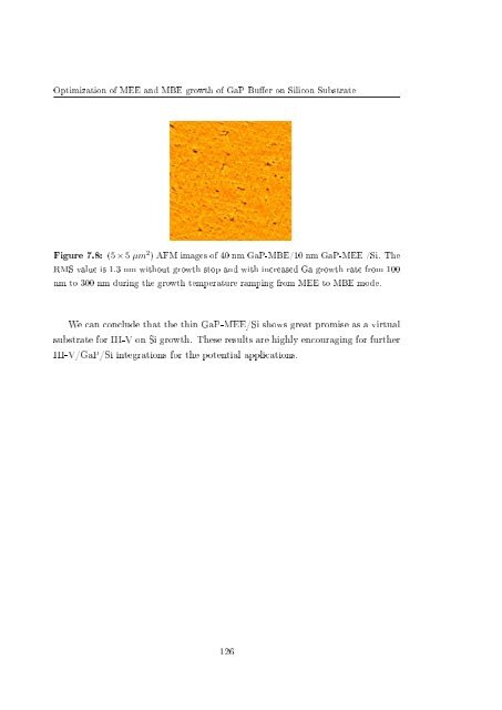
- Page 138 and 139: Optimization of MEE and MBE growth
- Page 142 and 143: Conclusions substrates, respectivel
- Page 144 and 145: REFERENCES [8] J. M. Gerard, O. Cab
- Page 146 and 147: REFERENCES [29] http://www.wmi.badw
- Page 148 and 149: REFERENCES [49] M. R. Brenner: GaP/
- Page 150 and 151: REFERENCES [66] Y. Ishida, T. Takah
- Page 152 and 153: REFERENCES [84] A. Garcia, C. M. Ma
- Page 154 and 155: REFERENCES [100] M. Felici, P. Gall
- Page 156 and 157: REFERENCES [116] H. Usui, H. Yasuda
- Page 158 and 159: REFERENCES [133] Grassman, T. J. Br
- Page 160 and 161: Conferences Contributions: Tariq Al
- Page 162 and 163: Nomenclature
- Page 164 and 165: REFERENCES symbol Descriptions γ f
- Page 166 and 167: like to thank all member of the Ins
- Page 168: REFERENCES Erklärung Hiermit versi