

Molecular beam epitaxial growth of III-V semiconductor ... - KOBRA
Molecular beam epitaxial growth of III-V semiconductor ... - KOBRA
Molecular beam epitaxial growth of III-V semiconductor ... - KOBRA

Create successful ePaper yourself
Turn your PDF publications into a flip-book with our unique Google optimized e-Paper software.
7.5 Optimization <strong>of</strong> MEE Followed by MBE Growth <strong>of</strong> GaP Buer on Si Substrate<br />
Streaky RHEED pattern was observed during MEE-GaP <strong>growth</strong> till the rst<br />
stage <strong>of</strong> MBE-GaP <strong>growth</strong> step indicating a 2D planar <strong>growth</strong> scenario for the<br />
rst 10 nm GaP-MEE as shown in Fig. 7.4(a). Streaky RHEED patterns were<br />
observed during the temperature ramping from 350 ◦ C till the MBE <strong>growth</strong> temperature<br />
<strong>of</strong> 560 ◦ C. At the GaP-MBE <strong>growth</strong> temperature and after a few nm<br />
GaP depositions spotty RHEED patterns are observed indicating a non-planar<br />
<strong>growth</strong> (Fig. 7.4(a)). The transition from streaky to spotty RHEED patterns,<br />
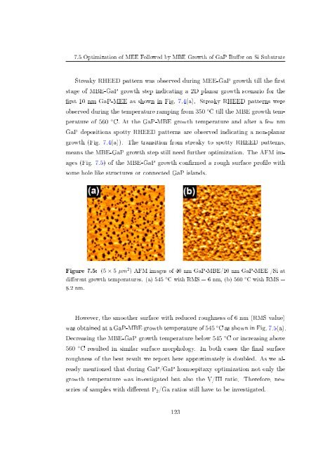
means the MBE-GaP <strong>growth</strong> step still need further optimization. The AFM images<br />
(Fig. 7.5) <strong>of</strong> the MBE-GaP <strong>growth</strong> conrmed a rough surface prole with<br />
some hole like structures or connected GaP islands.<br />
Figure 7.5:<br />
(5 × 5 µm 2 ) AFM images <strong>of</strong> 40 nm GaP-MBE/10 nm GaP-MEE /Si at<br />
dierent <strong>growth</strong> temperatures. (a) 545 ◦ C with RMS = 6 nm, (b) 560 ◦ C with RMS =<br />
8.2 nm.<br />
However, the smoother surface with reduced roughness <strong>of</strong> 6 nm (RMS value)<br />
was obtained at a GaP-MBE <strong>growth</strong> temperature <strong>of</strong> 545 ◦ C as shown in Fig. 7.5(a).<br />
Decreasing the MBE-GaP <strong>growth</strong> temperature below 545 ◦ C or increasing above<br />
560 ◦ C resulted in similar surface morphology. In both cases the nal surface<br />
roughness <strong>of</strong> the best result we report here approximately is doubled. As we already<br />
mentioned that during GaP/GaP homoepitaxy optimization not only the<br />
<strong>growth</strong> temperature was investigated but also the V/<strong>III</strong> ratio. Therefore, new<br />
series <strong>of</strong> samples with dierent P 2 /Ga ratios still have to be investigated.<br />
123


