

Molecular beam epitaxial growth of III-V semiconductor ... - KOBRA
Molecular beam epitaxial growth of III-V semiconductor ... - KOBRA
Molecular beam epitaxial growth of III-V semiconductor ... - KOBRA

Create successful ePaper yourself
Turn your PDF publications into a flip-book with our unique Google optimized e-Paper software.
MBE Growth <strong>of</strong> Self-Assembled InAs and InGaAs Quantum Dots Embedded in<br />
Silicon Matrix<br />
SiO 2 + 4Ga =⇒ Si + 2Ga 2 O (5.4)<br />
SiO 2 + 2Ga =⇒ SiO + Ga 2 O (5.5)<br />
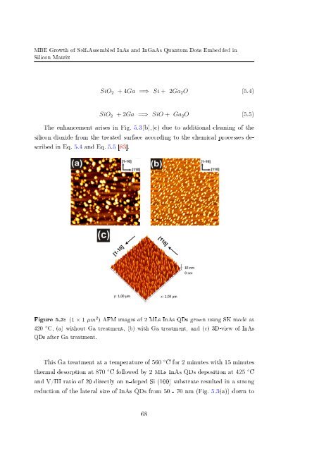
The enhancement arises in Fig. 5.3(b),(c) due to additional cleaning <strong>of</strong> the<br />
silicon dioxide from the treated surface according to the chemical processes described<br />
in Eq. 5.4 and Eq. 5.5 [83].<br />
Figure 5.3:<br />
(1 × 1 µm 2 ) AFM images <strong>of</strong> 2 MLs InAs QDs grown using SK mode at<br />
420 ◦ C, (a) without Ga treatment, (b) with Ga treatment, and (c) 3D-view <strong>of</strong> InAs<br />
QDs after Ga treatment.<br />
This Ga treatment at a temperature <strong>of</strong> 560 ◦ C for 2 minutes with 15 minutes<br />
thermal desorption at 870 ◦ C followed by 2 MLs InAs QDs deposition at 425 ◦ C<br />
and V/<strong>III</strong> ratio <strong>of</strong> 20 directly on n-doped Si (100) substrate resulted in a strong<br />
reduction <strong>of</strong> the lateral size <strong>of</strong> InAs QDs from 50 - 70 nm (Fig. 5.3(a)) down to<br />
68


