

Molecular beam epitaxial growth of III-V semiconductor ... - KOBRA
Molecular beam epitaxial growth of III-V semiconductor ... - KOBRA
Molecular beam epitaxial growth of III-V semiconductor ... - KOBRA

Create successful ePaper yourself
Turn your PDF publications into a flip-book with our unique Google optimized e-Paper software.
3.4 Challenges <strong>of</strong> Hetero<strong>epitaxial</strong> Growth <strong>of</strong> <strong>III</strong>-V on Silicon<br />
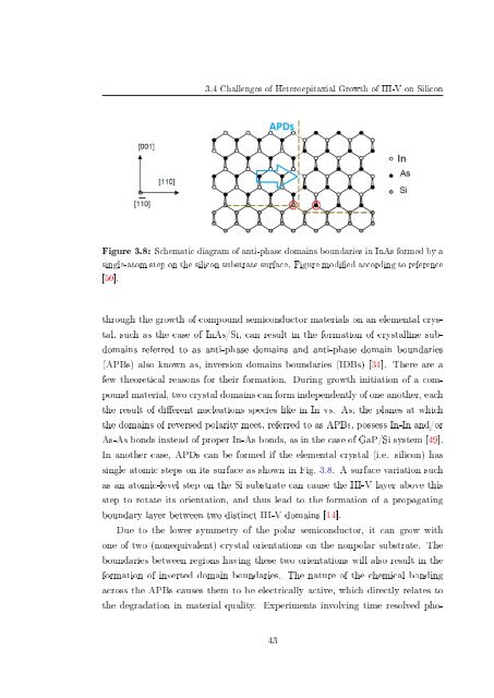
Figure 3.8: Schematic diagram <strong>of</strong> anti-phase domains boundaries in InAs formed by a<br />
single-atom step on the silicon substrate surface. Figure modied according to reference<br />
[50].<br />
through the <strong>growth</strong> <strong>of</strong> compound <strong>semiconductor</strong> materials on an elemental crystal,<br />
such as the case <strong>of</strong> InAs/Si, can result in the formation <strong>of</strong> crystalline subdomains<br />
referred to as anti-phase domains and anti-phase domain boundaries<br />
(APBs) also known as, inversion domains boundaries (IDBs) [31]. There are a<br />
few theoretical reasons for their formation. During <strong>growth</strong> initiation <strong>of</strong> a compound<br />
material, two crystal domains can form independently <strong>of</strong> one another, each<br />
the result <strong>of</strong> dierent nucleations species like in In vs. As; the planes at which<br />
the domains <strong>of</strong> reversed polarity meet, referred to as APBs, possess In-In and/or<br />
As-As bonds instead <strong>of</strong> proper In-As bonds, as in the case <strong>of</strong> GaP/Si system [49].<br />
In another case, APDs can be formed if the elemental crystal (i.e. silicon) has<br />
single atomic steps on its surface as shown in Fig. 3.8. A surface variation such<br />
as an atomic-level step on the Si substrate can cause the <strong>III</strong>-V layer above this<br />
step to rotate its orientation, and thus lead to the formation <strong>of</strong> a propagating<br />
boundary layer between two distinct <strong>III</strong>-V domains [14].<br />
Due to the lower symmetry <strong>of</strong> the polar <strong>semiconductor</strong>, it can grow with<br />
one <strong>of</strong> two (nonequivalent) crystal orientations on the nonpolar substrate. The<br />
boundaries between regions having these two orientations will also result in the<br />
formation <strong>of</strong> inverted domain boundaries. The nature <strong>of</strong> the chemical bonding<br />
across the APBs causes them to be electrically active, which directly relates to<br />
the degradation in material quality. Experiments involving time resolved pho-<br />
43


