

Molecular beam epitaxial growth of III-V semiconductor ... - KOBRA
Molecular beam epitaxial growth of III-V semiconductor ... - KOBRA
Molecular beam epitaxial growth of III-V semiconductor ... - KOBRA

Create successful ePaper yourself
Turn your PDF publications into a flip-book with our unique Google optimized e-Paper software.
Hetero<strong>epitaxial</strong> Growth <strong>of</strong> <strong>III</strong>-V Semiconductor on Silicon Substrates<br />
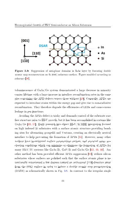
Figure 3.9:<br />
Suppression <strong>of</strong> anti-phase domains in InAs layer by featuring double<br />
atomic step reconstruction on Si (001) substrate surface. Figure modied according to<br />
reference [50].<br />
toluminescence <strong>of</strong> GaAs/Ge system demonstrated a large decrease in minority<br />
carrier lifetime with a large increase in interface recombination rates in the samples<br />
containing the APD defects versus those without [49]. Generally, APDs are<br />
expected to introduce states within the energy gap and give rise to non-radiative<br />
recombination. They therefore degrade the eciencies <strong>of</strong> LEDs and cause excess<br />
leakage in p-n junctions.<br />
Avoiding the APDs defect is tricky and demands control <strong>of</strong> the substrate surface<br />
structure prior to <strong>III</strong>-V <strong>growth</strong>, but it has been accomplished in systems like<br />
GaAs/Ge [60, 57]. Early research into direct <strong>III</strong>-V/Si MBE integration focused<br />
on high indexed Si substrates with a surface atomic structure providing bonding<br />
sites for alternating group-<strong>III</strong> and V-atoms, creating an electrically neutral<br />
interface to help preventing the formation <strong>of</strong> APDs [61]. However, many other<br />
authors have investigated surface preparations recipes, and reported many nucleation<br />
conditions which can minimize or eliminate the formation <strong>of</strong> APDs for<br />
many <strong>III</strong>-V/IV systems like GaAs/Si, GaP/Si and GaAs/Ge [62, 49, 60]. Another<br />
method has been provided ecient APDs suppression [63], utilizes silicon<br />
substrates whose surfaces are polished such that the surface atomic plane is intentionally<br />
misoriented a few degrees toward an orthogonal [110] direction away<br />
from the (001) surface in order to induce a double atomic step reconstruction<br />
(DASR) as schematically shown in Fig. 3.9. In contrast to the irregular single<br />
44


