

Molecular beam epitaxial growth of III-V semiconductor ... - KOBRA
Molecular beam epitaxial growth of III-V semiconductor ... - KOBRA
Molecular beam epitaxial growth of III-V semiconductor ... - KOBRA

Create successful ePaper yourself
Turn your PDF publications into a flip-book with our unique Google optimized e-Paper software.
MBE Growth <strong>of</strong> Self-Assembled InAs and InGaAs Quantum Dots Embedded in<br />
Silicon Matrix<br />
reconstruction with bubbles (spherical or circular-voids without material inside)<br />
and vacancy stacking faults (V-SF) formation above the InAs QDs has been<br />
observed. The vacancy SFs and circular-voids formation are very logical traces <strong>of</strong><br />
the possible route <strong>of</strong> lling the voids. The dark eld cross-section TEM image <strong>of</strong><br />
the grown structure in Fig. 5.17(b) shows the InAs QDs with a missing wetting<br />
layer and the shape transition evolution from pyramidal and at to spherical and<br />
faceted dots. The V-SF and the circular-voids above the InAs QDs are clearly<br />
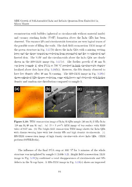
shown in the HR-TEM image Fig. 5.17(c). The further <strong>growth</strong> <strong>of</strong> 40 nm Si<br />
cap layer (sample 4) after PGA at 700 ◦ C resulted in high circular-voids density<br />
localized above dots layer (Fig. 5.18(b)). However, the SFs density observed to<br />
have low density after 40 nm Si capping. The HR-TEM image in Fig. 5.18(c)<br />
shows spherical QDs shapes evolution, some with facets and obviously with higher<br />
density and random size distribution compared to sample 3.<br />
Figure 5.18: TEM cross-section image <strong>of</strong> InAs/Si QDs sample (50 nm Si/2 MLs InAs<br />
/10 nm Si/40 nm Si cap). (a) (3 × 3 µm 2 ) AFM image <strong>of</strong> top surface with RMS<br />
value <strong>of</strong> 0.37 nm. (b) The bright eld cross-section TEM image shows the InAs QDs<br />
with dismiss wetting layer with low density SFs and high density circular-voids. (c)<br />
HR-TEM cross-section image <strong>of</strong> high density circular-voids above InAs QDs. (TEM<br />
performed@PDI-Berlin).<br />
The inuence <strong>of</strong> the nal PGA step at 800 ◦ C for 5 minutes <strong>of</strong> the whole<br />
structure was invigilated by sample 5 (Table 5.2). Bright eld cross-section TEM<br />
image in Fig. 5.19(b) conrmed a total disappearance <strong>of</strong> circular-voids and SFs<br />
defects in the Si cap layer. A HR-TEM image in Fig. 5.19(c) shows an improved<br />
84


