

Molecular beam epitaxial growth of III-V semiconductor ... - KOBRA
Molecular beam epitaxial growth of III-V semiconductor ... - KOBRA
Molecular beam epitaxial growth of III-V semiconductor ... - KOBRA

Create successful ePaper yourself
Turn your PDF publications into a flip-book with our unique Google optimized e-Paper software.
7.4 MEE Growth <strong>of</strong> GaP Buer on Si Substrate<br />
as described in Sec. 7.3. The samples were then cooled-down to 350 ◦ C for MEE<br />
<strong>growth</strong>. MEE was conducted by using a 100 nm/h gallium <strong>growth</strong> rate for the Ga<br />
deposition, while the P 2 ux was set to ∼ 15x the Ga ux, with samples produced<br />
utilizing both Ga and P 2 initiation [133, 49]. While the P 2 ux pulse was not<br />
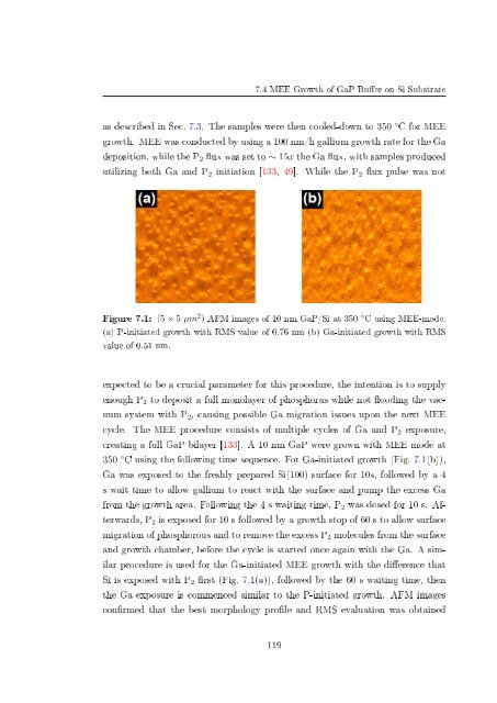
Figure 7.1: (5 × 5 µm 2 ) AFM images <strong>of</strong> 10 nm GaP/Si at 350 ◦ C using MEE-mode.<br />
(a) P-initiated <strong>growth</strong> with RMS value <strong>of</strong> 0.76 nm (b) Ga-initiated <strong>growth</strong> with RMS<br />
value <strong>of</strong> 0.51 nm.<br />
expected to be a crucial parameter for this procedure, the intention is to supply<br />
enough P 2 to deposit a full monolayer <strong>of</strong> phosphorus while not ooding the vacuum<br />
system with P 2 , causing possible Ga migration issues upon the next MEE<br />
cycle. The MEE procedure consists <strong>of</strong> multiple cycles <strong>of</strong> Ga and P 2 exposure,<br />
creating a full GaP bilayer [133]. A 10 nm GaP were grown with MEE mode at<br />
350 ◦ C using the following time sequence. For Ga-initiated <strong>growth</strong> (Fig. 7.1(b)),<br />
Ga was exposed to the freshly prepared Si(100) surface for 10s, followed by a 4<br />
s wait time to allow gallium to react with the surface and pump the excess Ga<br />
from the <strong>growth</strong> area. Following the 4 s waiting time, P 2 was dosed for 10 s. Afterwards,<br />
P 2 is exposed for 10 s followed by a <strong>growth</strong> stop <strong>of</strong> 60 s to allow surface<br />
migration <strong>of</strong> phosphorous and to remove the excess P 2 molecules from the surface<br />
and <strong>growth</strong> chamber, before the cycle is started once again with the Ga. A similar<br />
procedure is used for the Ga-initiated MEE <strong>growth</strong> with the dierence that<br />
Si is exposed with P 2 rst (Fig. 7.1(a)), followed by the 60 s waiting time, then<br />
the Ga exposure is commenced similar to the P-initiated <strong>growth</strong>. AFM images<br />
conrmed that the best morphology prole and RMS evaluation was obtained<br />
119


