

Molecular beam epitaxial growth of III-V semiconductor ... - KOBRA
Molecular beam epitaxial growth of III-V semiconductor ... - KOBRA
Molecular beam epitaxial growth of III-V semiconductor ... - KOBRA

You also want an ePaper? Increase the reach of your titles
YUMPU automatically turns print PDFs into web optimized ePapers that Google loves.
MBE Growth <strong>of</strong> Self-Assembled InAs and InGaAs Quantum Dots Embedded in<br />
Silicon Matrix<br />
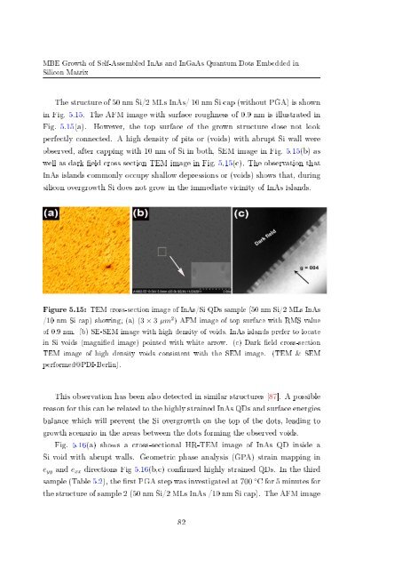
The structure <strong>of</strong> 50 nm Si/2 MLs InAs/ 10 nm Si cap (without PGA) is shown<br />
in Fig. 5.15. The AFM image with surface roughness <strong>of</strong> 0.9 nm is illustrated in<br />
Fig. 5.15(a). However, the top surface <strong>of</strong> the grown structure dose not look<br />
perfectly connected. A high density <strong>of</strong> pits or (voids) with abrupt Si wall were<br />
observed, after capping with 10 nm <strong>of</strong> Si in both, SEM image in Fig. 5.15(b) as<br />
well as dark eld cross section TEM image in Fig. 5.15(c). The observation that<br />
InAs islands commonly occupy shallow depressions or (voids) shows that, during<br />
silicon over<strong>growth</strong> Si does not grow in the immediate vicinity <strong>of</strong> InAs islands.<br />
Figure 5.15: TEM cross-section image <strong>of</strong> InAs/Si QDs sample (50 nm Si/2 MLs InAs<br />
/10 nm Si cap) showing; (a) (3 × 3 µm 2 ) AFM image <strong>of</strong> top surface with RMS value<br />
<strong>of</strong> 0.9 nm. (b) SE-SEM image with high density <strong>of</strong> voids, InAs islands prefer to locate<br />
in Si voids (magnied image) pointed with white arrow. (c) Dark eld cross-section<br />
TEM image <strong>of</strong> high density voids consistent with the SEM image. (TEM & SEM<br />
performed@PDI-Berlin).<br />
This observation has been also detected in similar structures [87]. A possible<br />
reason for this can be related to the highly strained InAs QDs and surface energies<br />
balance which will prevent the Si over<strong>growth</strong> on the top <strong>of</strong> the dots, leading to<br />
<strong>growth</strong> scenario in the areas between the dots forming the observed voids.<br />
Fig. 5.16(a) shows a cross-sectional HR-TEM image <strong>of</strong> InAs QD inside a<br />
Si void with abrupt walls. Geometric phase analysis (GPA) strain mapping in<br />
e yy and e xx directions Fig 5.16(b,c) conrmed highly strained QDs. In the third<br />
sample (Table 5.2), the rst PGA step was investigated at 700 ◦ C for 5 minutes for<br />
the structure <strong>of</strong> sample 2 (50 nm Si/2 MLs InAs /10 nm Si cap). The AFM image<br />
82


