

Molecular beam epitaxial growth of III-V semiconductor ... - KOBRA
Molecular beam epitaxial growth of III-V semiconductor ... - KOBRA
Molecular beam epitaxial growth of III-V semiconductor ... - KOBRA

Create successful ePaper yourself
Turn your PDF publications into a flip-book with our unique Google optimized e-Paper software.
7.5 Optimization <strong>of</strong> MEE Followed by MBE Growth <strong>of</strong> GaP Buer on Si Substrate<br />
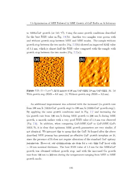
to MBE-GaP <strong>growth</strong> (at 545 ◦ C). Using the same <strong>growth</strong> conditions described<br />
for the best RMS value in Fig. 7.6(b). Another two samples were grown with<br />
and without <strong>growth</strong> stop between MEE and MBE modes. The sample without<br />
<strong>growth</strong> stop between the two modes (Fig. 7.7(b)) showed an improved RMS value<br />
<strong>of</strong> 3.2 nm, which is almost half the RMS value compared with the sample with<br />
<strong>growth</strong> stop between the two modes (Fig. 7.7(a)).<br />
Figure 7.7: (5 × 5 µm 2 ) AFM images <strong>of</strong> 40 nm GaP-MBE/10 nm GaP-MEE /Si. (a)<br />
With <strong>growth</strong> stop (RMS = 6.8 nm). (b) Without <strong>growth</strong> stop (RMS = 3.2 nm).<br />
An additional improvement was achieved with the increased Ga <strong>growth</strong> rate<br />
from 100 nm/h (MEE-GaP <strong>growth</strong> step) to 300 nm/h (MBE-GaP <strong>growth</strong> step)).<br />
By applying the same <strong>growth</strong> conditions used in Fig. 7.7 and increasing the<br />
Ga <strong>growth</strong> rate from 100 nm/h during MEE <strong>growth</strong> to 300 nm/h during MBE<br />
<strong>growth</strong>, a smooth surface with a very good RMS value <strong>of</strong> 1.3 nm was observed<br />
(Fig. 7.8). In addition, when comparing GaP-MBE/GaP to GaP-MBE/GaP-<br />
MEE/Si, it is clear that optimum MBE <strong>growth</strong> parameters are very similar, if<br />
not identical. We interpret this to mean that the GaP/Si formed after the above<br />
described MEE process has generated an eective GaP <strong>growth</strong> template on Si,<br />
since the presence <strong>of</strong> Si does not require alteration <strong>of</strong> the standard GaP epitaxy<br />
parameters. However, our optimizations are done for a very thin GaP layer with<br />
∼ 50 nm nominal thickness. The best RMS value <strong>of</strong> 1.3 nm for the MBE-GaP<br />
<strong>growth</strong> was obtained without <strong>growth</strong> stop, and with the increased Ga <strong>growth</strong><br />
rate from 100 nm to 300 nm during the temperature ramping from MEE to MBE<br />
<strong>growth</strong> mode.<br />
125


