

Molecular beam epitaxial growth of III-V semiconductor ... - KOBRA
Molecular beam epitaxial growth of III-V semiconductor ... - KOBRA
Molecular beam epitaxial growth of III-V semiconductor ... - KOBRA

You also want an ePaper? Increase the reach of your titles
YUMPU automatically turns print PDFs into web optimized ePapers that Google loves.
MBE Growth <strong>of</strong> Self-Assembled InAs and InGaAs Quantum Dots Embedded in<br />
Silicon Matrix<br />
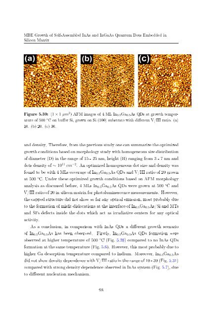
Figure 5.30: (1 × 1 µm 2 ) AFM images <strong>of</strong> 4 ML In 0.5 Ga 0.5 As QDs at <strong>growth</strong> temperature<br />
<strong>of</strong> 500 ◦ C on buer Si, grown on Si (100) substrate with dierent V/<strong>III</strong> ratio. (a)<br />
10. (b) 20. (c) 30.<br />
and density. Therefore, from the previous study one can summarize the optimized<br />
<strong>growth</strong> conditions based on morphology study with homogeneous size distribution<br />
<strong>of</strong> diameter (D) in the range <strong>of</strong> 15 - 25 nm, height (H) ranging from 3 - 7 nm and<br />
dots density <strong>of</strong> ∼ 10 11 cm −2 . An optimized homogeneous dot size and density was<br />
found to be with 4 MLs coverage <strong>of</strong> In 0.5 Ga 0.5 As QDs and V/<strong>III</strong> ratio <strong>of</strong> 20 grown<br />
at 500 ◦ C. Under these optimized <strong>growth</strong> conditions based on AFM morphology<br />
analysis as discussed before, 4 MLs In 0.5 Ga 0.5 As QDs were grown at 500 ◦ C and<br />
V/<strong>III</strong> ratio <strong>of</strong> 20 in silicon matrix for photoluminescence measurements. However,<br />
the capped structure did not show so far any optical emission, most probably due<br />
to the formation <strong>of</strong> mist dislocations at the interface <strong>of</strong> In 0.5 Ga 0.5 As/Si and MTs<br />
and SFs defects inside the dots which act as irradiative centers for any optical<br />
activity.<br />
As a conclusion, in comparison with InAs QDs a dierent <strong>growth</strong> scenario<br />
<strong>of</strong> In 0.5 Ga 0.5 As has been observed. Firstly, In 0.5 Ga 0.5 As QDs formation were<br />
observed at higher temperature <strong>of</strong> 500 ◦ C (Fig. 5.28) compared to no InAs QDs<br />
formation at the same temperature (Fig. 5.6). However, this most probably due to<br />
higher Ga desorption temperature compared to Indium. Moreover, In 0.5 Ga 0.5 As<br />
did not show density dependence with V/<strong>III</strong> ratio in the range <strong>of</strong> 10 - 30 (Fig. 5.31)<br />
compared with strong density dependence observed in InAs system (Fig. 5.7), due<br />
to dierent nucleation mechanism.<br />
98


