

Molecular beam epitaxial growth of III-V semiconductor ... - KOBRA
Molecular beam epitaxial growth of III-V semiconductor ... - KOBRA
Molecular beam epitaxial growth of III-V semiconductor ... - KOBRA

Create successful ePaper yourself
Turn your PDF publications into a flip-book with our unique Google optimized e-Paper software.
7.5 Optimization <strong>of</strong> MEE Followed by MBE Growth <strong>of</strong> GaP Buer on Si Substrate<br />
7.4.2 MEE - P 2 /Ga Ratio<br />
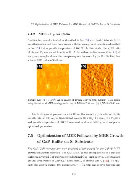
Another two samples treated as described in Sec. 7.3 were loaded into the MBE<br />
<strong>growth</strong> chamber and have been grown with the same <strong>growth</strong> conditions described<br />
in Sec. 7.4.1 at a <strong>growth</strong> temperature <strong>of</strong> 350 ◦ C. In this study, the V/<strong>III</strong> ratio<br />
<strong>of</strong> Ga and P 2 was varied from 5 to 15. AFM surface prole images (Fig. 7.3) <strong>of</strong><br />
the grown samples shows that sample exposed by more P 2 (∼ 15x Ga ux) has<br />
a lower RMS value <strong>of</strong> 0.46 nm.<br />
Figure 7.3:<br />
(1 × 1 µm 2 ) AFM images <strong>of</strong> 10 nm GaP/Si with dierent V/<strong>III</strong> ratios<br />
using Ga-initiated MEE-mode <strong>growth</strong>. (a) 15, RMS <strong>of</strong> 0.46 nm, (b) 5, RMS <strong>of</strong> 0.82 nm.<br />
The MEE <strong>growth</strong> parameters with 10 nm thickness, P 2 /Ga ratio <strong>of</strong> 15, Ga<br />
<strong>growth</strong> rate <strong>of</strong> 100 nm/h, Ga-initiated <strong>growth</strong> 10 s Ga/ 4 s stop/10 s P 2 /60 s<br />
and <strong>growth</strong> temperature <strong>of</strong> 350 ◦ C were used in all next MEE <strong>growth</strong> recipes as<br />
optimized parameters.<br />
7.5 Optimization <strong>of</strong> MEE Followed by MBE Growth<br />
<strong>of</strong> GaP Buer on Si Substrate<br />
The GaP/GaP homoepitaxy work provided a background for the GaP/Si MBE<br />
<strong>growth</strong> parameters selection. The GaP-MEE/Si was anticipated to be a suitable<br />
surface as a virtual GaP substrate for additional GaP-MBE <strong>growth</strong>. The standard<br />
<strong>growth</strong> temperature <strong>of</strong> GaP/GaP homoepitaxy is around 550 ◦ C [136]. To optimize<br />
this <strong>growth</strong> regime, two parameters, P 2 /Ga ratio and <strong>growth</strong> temperature<br />
121


