

Molecular beam epitaxial growth of III-V semiconductor ... - KOBRA
Molecular beam epitaxial growth of III-V semiconductor ... - KOBRA
Molecular beam epitaxial growth of III-V semiconductor ... - KOBRA

You also want an ePaper? Increase the reach of your titles
YUMPU automatically turns print PDFs into web optimized ePapers that Google loves.
MBE Growth <strong>of</strong> Self-Assembled InAs and InGaAs Quantum Dots Embedded in<br />
Silicon Matrix<br />
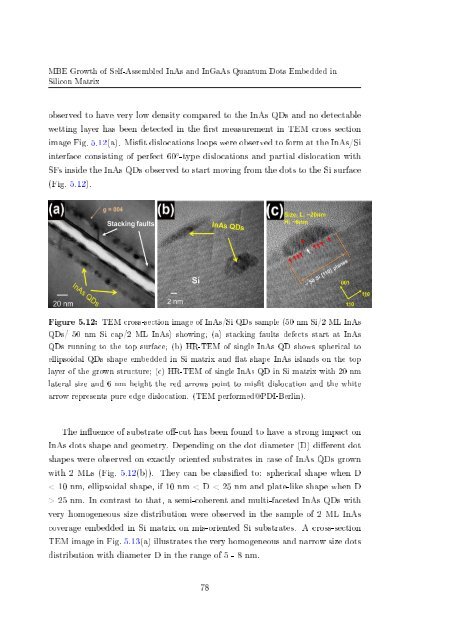
observed to have very low density compared to the InAs QDs and no detectable<br />
wetting layer has been detected in the rst measurement in TEM cross section<br />
image Fig. 5.12(a). Mist dislocations loops were observed to form at the InAs/Si<br />
interface consisting <strong>of</strong> perfect 60 ◦ -type dislocations and partial dislocation with<br />
SFs inside the InAs QDs observed to start moving from the dots to the Si surface<br />
(Fig. 5.12).<br />
Figure 5.12: TEM cross-section image <strong>of</strong> InAs/Si QDs sample (50 nm Si/2 ML InAs<br />
QDs/ 50 nm Si cap/2 ML InAs) showing; (a) stacking faults defects start at InAs<br />
QDs running to the top surface; (b) HR-TEM <strong>of</strong> single InAs QD shows spherical to<br />
ellipsoidal QDs shape embedded in Si matrix and at shape InAs islands on the top<br />
layer <strong>of</strong> the grown structure; (c) HR-TEM <strong>of</strong> single InAs QD in Si matrix with 20 nm<br />
lateral size and 6 nm height the red arrows point to mist dislocation and the white<br />
arrow represents pure edge dislocation. (TEM performed@PDI-Berlin).<br />
The inuence <strong>of</strong> substrate o-cut has been found to have a strong impact on<br />
InAs dots shape and geometry. Depending on the dot diameter (D) dierent dot<br />
shapes were observed on exactly oriented substrates in case <strong>of</strong> InAs QDs grown<br />
with 2 MLs (Fig. 5.12(b)). They can be classied to: spherical shape when D<br />
< 10 nm, ellipsoidal shape, if 10 nm < D < 25 nm and plate-like shape when D<br />
> 25 nm. In contrast to that, a semi-coherent and multi-faceted InAs QDs with<br />
very homogeneous size distribution were observed in the sample <strong>of</strong> 2 ML InAs<br />
coverage embedded in Si matrix on mis-oriented Si substrates. A cross-section<br />
TEM image in Fig. 5.13(a) illustrates the very homogeneous and narrow size dots<br />
distribution with diameter D in the range <strong>of</strong> 5 - 8 nm.<br />
78


