

Molecular beam epitaxial growth of III-V semiconductor ... - KOBRA
Molecular beam epitaxial growth of III-V semiconductor ... - KOBRA
Molecular beam epitaxial growth of III-V semiconductor ... - KOBRA

You also want an ePaper? Increase the reach of your titles
YUMPU automatically turns print PDFs into web optimized ePapers that Google loves.
MBE Growth <strong>of</strong> Self-Assembled InAs and InGaAs Quantum Dots Embedded in<br />
Silicon Matrix<br />
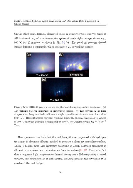
On the other hand, RHEED elongated spots in semicircle were observed without<br />
AH treatment only after a thermal desorption at much higher temperatures (e.g.,<br />
900 ◦ C for 15 minutes as shown in Fig. 5.1(b). The resulting pattern showed<br />
streaks forming a semicircle, which indicates a 2D crystalline surface.<br />
Figure 5.1:<br />
RHEED pattern during the thermal desorption surface treatment. (a)<br />
The diusive pattern indicating an amorphous surface. (b) The pattern in the form<br />
<strong>of</strong> spots describing semicircle indicates a single crystalline surface and was observed at<br />
900 ◦ C. (c) RHEED pattern (streaks) resulting during the thermal desorption treatment<br />
at 700 ◦ C after the hydrogen cleaning step at 500 ◦ C for 45 minutes with P H = 3×10 −7<br />
Torr.<br />
Hence, one can conclude that thermal desorption accompanied with hydrogen<br />
treatment is the most ecient method to prepare a clean 2D crystalline surface,<br />
which is in agreement with literature according to which hydrogen treatment is<br />
ecient to remove carbon contamination from the surface [81, 82]. Due to the fact<br />
that a long time high temperatures thermal desorption will destroy pre-patterned<br />
surfaces, like nanoholes, an in-situ thermal cleaning process was developed with<br />
a reduced thermal budget.<br />
66


