

Molecular beam epitaxial growth of III-V semiconductor ... - KOBRA
Molecular beam epitaxial growth of III-V semiconductor ... - KOBRA
Molecular beam epitaxial growth of III-V semiconductor ... - KOBRA

You also want an ePaper? Increase the reach of your titles
YUMPU automatically turns print PDFs into web optimized ePapers that Google loves.
5.4 Self-Assembled InAs QDs Embedded in Si Matrix<br />
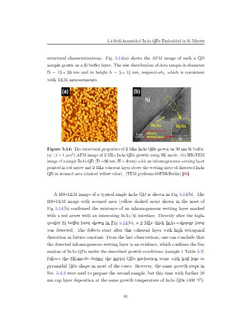
structural characterizations. Fig. 5.14(a) shows the AFM image <strong>of</strong> such a QD<br />
sample grown on a Si buer layer. The size distribution <strong>of</strong> dots ranges in diameter<br />
D = 15 - 30 nm and in height h = 5 - 15 nm, respectively, which is consistent<br />
with TEM measurements.<br />
Figure 5.14: The structural properties <strong>of</strong> 2 MLs InAs QDs grown on 50 nm Si buer.<br />
(a) (1 × 1 µm 2 ) AFM image <strong>of</strong> 2 MLs InAs QDs <strong>growth</strong> using SK mode. (b) HR-TEM<br />
image <strong>of</strong> a single InAs QD (D =20 nm, H = 9 nm) with an inhomogeneous wetting layer<br />
pointed in red arrow and 2 MLs coherent layer above the wetting layer <strong>of</strong> distorted InAs<br />
QD in zoomed area (dashed yellow color). (TEM performed@PDI-Berlin) [86].<br />
A HR-TEM image <strong>of</strong> a typical single InAs QD is shown in Fig 5.14(b). The<br />
HR-TEM image with zoomed area (yellow dashed area) shown in the inset <strong>of</strong><br />
Fig 5.14(b) conrmed the existence <strong>of</strong> an inhomogeneous wetting layer marked<br />
with a red arrow with an interesting InAs/Si interface. Directly after the highquality<br />
Si buer layer shown in Fig 5.14(b), a 2 MLs thick InAs coherent layer<br />
was detected. The defects start after this coherent layer with high tetragonal<br />
distortion in lattice constant. From the last observations, one can conclude that<br />
the detected inhomogeneous wetting layer is an evidence, which conrms the formation<br />
<strong>of</strong> InAs QDs under the described <strong>growth</strong> conditions (sample 1 Table 5.2)<br />
follows the SK-mode during the initial QDs nucleation stage with half lens to<br />
pyramidal QDs shape in most <strong>of</strong> the cases. However, the same <strong>growth</strong> steps in<br />
Sec. 5.4.3 were used to prepare the second sample, but this time with further 10<br />
nm cap layer deposition at the same <strong>growth</strong> temperature <strong>of</strong> InAs QDs (400 ◦ C).<br />
81


