

Molecular beam epitaxial growth of III-V semiconductor ... - KOBRA
Molecular beam epitaxial growth of III-V semiconductor ... - KOBRA
Molecular beam epitaxial growth of III-V semiconductor ... - KOBRA

Create successful ePaper yourself
Turn your PDF publications into a flip-book with our unique Google optimized e-Paper software.
5.4 Self-Assembled InAs QDs Embedded in Si Matrix<br />
ramping rate <strong>of</strong> 50 K/min for the <strong>growth</strong> <strong>of</strong> further 40 nm <strong>of</strong> Si to form nally<br />
a 50 nm thick cap layer in two <strong>growth</strong> steps. At the nal stage, another 10<br />
minutes PGA was performed to improve the crystallinity <strong>of</strong> the whole structure.<br />
Fig. 5.10(a) shows the band structure scheme <strong>of</strong> the intended grown structure<br />
(Si/InAs/Si/InAs), while Fig. 5.10(b) shows the layer scheme <strong>of</strong> the same structure.<br />
The top InAs QDs layer was grown for AFM characterization and the sandwiched<br />
(buried) InAs layer for PL characterization. The <strong>growth</strong> conditions <strong>of</strong> SA<br />
InAs QDs used for the preparation <strong>of</strong> the two series are: V/<strong>III</strong> = 25, T G = 400 ◦ C,<br />
In <strong>growth</strong> rate = 108 nm/h (0.1 ML/s) with dierent nominal thickness <strong>of</strong> 1, 2<br />
or 4 MLs InAs QDs.<br />
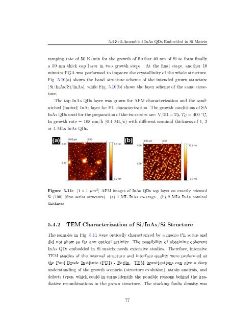
Figure 5.11:<br />
(1 × 1 µm 2 ) AFM images <strong>of</strong> InAs QDs top layer on exactly oriented<br />
Si (100) (rst series structure). (a) 1 ML InAs coverage , (b) 2 MLs InAs nominal<br />
thickness.<br />
5.4.2 TEM Characterization <strong>of</strong> Si/InAs/Si Structure<br />
The samples in Fig. 5.11 were optically characterized by a macro PL setup and<br />
did not show so far any optical activity. The possibility <strong>of</strong> obtaining coherent<br />
InAs QDs embedded in Si matrix needs extensive studies. Therefore, intensive<br />
TEM studies <strong>of</strong> the internal structure and interface quality were preformed at<br />
the Paul Drude Institute (PDI) - Berlin. TEM investigations can give a deep<br />
understanding <strong>of</strong> the <strong>growth</strong> scenario (structure evolution), strain analysis, and<br />
defects types, which could in turns identify the possible reasons behind the irradiative<br />
recombinations in the grown structure. The stacking faults density was<br />
77


