xxiii Ïανελληνιο ÏÏ Î½ÎµÎ´Ïιο ÏÏ ÏÎ¹ÎºÎ·Ï ÏÏεÏÎµÎ±Ï ÎºÎ±ÏαÏÏαÏÎ·Ï & εÏιÏÏÎ·Î¼Î·Ï ...
xxiii Ïανελληνιο ÏÏ Î½ÎµÎ´Ïιο ÏÏ ÏÎ¹ÎºÎ·Ï ÏÏεÏÎµÎ±Ï ÎºÎ±ÏαÏÏαÏÎ·Ï & εÏιÏÏÎ·Î¼Î·Ï ...
xxiii Ïανελληνιο ÏÏ Î½ÎµÎ´Ïιο ÏÏ ÏÎ¹ÎºÎ·Ï ÏÏεÏÎµÎ±Ï ÎºÎ±ÏαÏÏαÏÎ·Ï & εÏιÏÏÎ·Î¼Î·Ï ...

You also want an ePaper? Increase the reach of your titles
YUMPU automatically turns print PDFs into web optimized ePapers that Google loves.
Annealing Induced Dissociation of N 2 Formed in Indium Implanted GaN<br />
M. Katsikini 1* , E. C. Paloura 1 , F. Boscherini 2 , E. Wendler 3 , W. Wesch 3 .<br />
1 Aristotle University of Thessaloniki, School of Physics, Section of Solid State Physics, 54124 Thessaloniki, Greece<br />
2<br />
Department of Physics and CNISM, University of Bologna, viale C. Berti Pichat 6/2, 40127 Bologna, Italy<br />
3<br />
Institut fur Festkörperphysik, Friedrich-Schiller Universität Jena, Max-Wien-Platz 1, 07743, Germany<br />
*katsiki@auth.gr<br />
InGaN/GaN heterostructures find applications in the fabrication of high efficiency light emitting diodes as well as in high –<br />
frequency, high – power microelectronic devices [1]. Ion implantation followed by annealing is a promising method for the<br />
growth of nanomaterials [2,3], like InGaN quantum dots, which enhance the emission characteristics of InGaN – based laser<br />
diodes [4], and InGaN/GaN heterostructures. For example, high dose Ge implantation in Si has been proposed as a method<br />
for the fabrication of Si x Ge y /Si heterostructures [5]. Although ion implantation has the advantage of precise dose and profile<br />
control, it causes lattice damage which can be recovered via annealing. Here, we apply near edge x-ray absorption fine<br />
structure (NEXAFS) spectroscopy at the N K edge, in order to determine the implantation induced changes in the electronic<br />
structure of GaN samples. XAFS spectroscopies are ideally suited for the study of highly defective or amorphous materials,<br />
such as implanted samples, since the main mechanism involved is the backscattering of the outgoing photoelectron wave<br />
from the neighboring atoms which does not depend on the periodicity of the lattice. More specifically, we focus on the<br />
identification and thermal stability of N 2 gaseous bubbles that have been proposed [6] as an implantation induced defect in<br />
ion implanted GaN.<br />
The 450nm – thick – GaN sample was grown on Al 2 O 3 by Plasma Enhanced Molecular Beam Epitaxy using an AlN<br />
buffer layer [7]. The sample was diced and the<br />
individual pieces were implanted at 77 K with<br />
700 keV In ions with a fluence of 5 × 10 15 cm -2 .<br />
Rutherford backscattering characterization has<br />
4<br />
shown that a 200 µm thick amorphous layer is<br />
formed on the surface of the sample, while the<br />
remaining GaN sample is severely defected.<br />
as grown<br />
The implanted samples were subjected to rapid<br />
thermal annealing (RTA) at 800 o and 900 o C<br />
for 15 sec. The N K edge NEXAFS<br />
3<br />
ann. (900 o C)<br />
measurements were conducted at the ALOISA<br />
undulator beamline of the Synchrotron<br />
Radiation facility ELETTRA in Trieste. The<br />
spectra were recorded in the fluorescence yield<br />
ann. (800 o C)<br />
mode using a high purity Ge detector cooled at<br />
RL<br />
77K. In order to avoid polarisation effects, the<br />
2<br />
angle of incidence was equal to the magic<br />
as implanted<br />
angle (55 o to the sample surface). The<br />
information depth of the fluorescence photons<br />
is approximately equal to 40nm.<br />
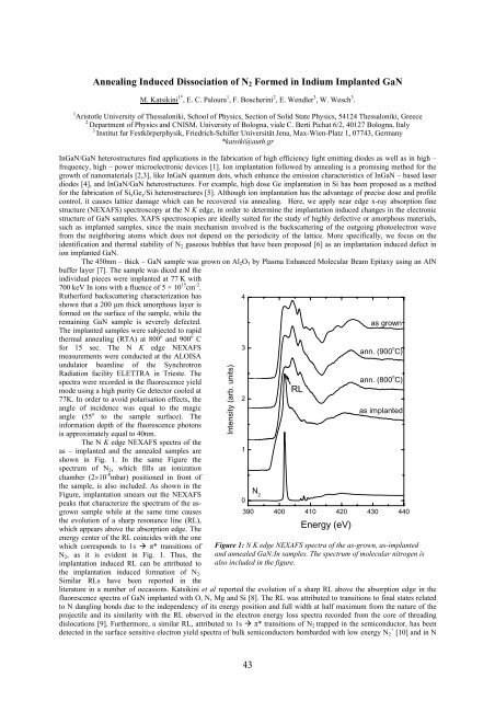
The N K edge NEXAFS spectra of the<br />
as – implanted and the annealed samples are<br />
shown in Fig. 1. In the same Figure the<br />
spectrum of N 2 , which fills an ionization<br />
chamber (2×10 -8 mbar) positioned in front of<br />
the sample, is also included. As shown in the<br />
Figure, implantation smears out the NEXAFS<br />
peaks that characterize the spectrum of the asgrown<br />
sample while at the same time causes<br />
the evolution of a sharp resonance line (RL),<br />
which appears above the absorption edge. The<br />
energy center of the RL coincides with the one<br />
which corresponds to 1s π * transitions of<br />
N 2 , as it is evident in Fig. 1. Thus, the<br />
implantation induced RL can be attributed to<br />
the implantation induced formation of N 2 .<br />
Similar RLs have been reported in the<br />
Intensity (arb. units)<br />
1<br />
0<br />
390 400 410 420 430 440<br />
Energy (eV)<br />
literature in a number of occasions. Katsikini et al reported the evolution of a sharp RL above the absorption edge in the<br />
fluorescence spectra of GaN implanted with O, N, Mg and Si [8]. The RL was attributed to transitions to final states related<br />
to N dangling bonds due to the independency of its energy position and full width at half maximum from the nature of the<br />
projectile and its similarity with the RL observed in the electron energy loss spectra recorded from the core of threading<br />
dislocations [9]. Furthermore, a similar RL, attributed to 1s π* transitions of N 2 trapped in the semiconductor, has been<br />
detected in the surface sensitive electron yield spectra of bulk semiconductors bombarded with low energy N 2 + [10] and in N<br />
N 2<br />
Figure 1: N K edge NEXAFS spectra of the as-grown, as-implanted<br />
and annealed GaN:In samples. The spectrum of molecular nitrogen is<br />
also included in the figure.<br />
43