xxiii Ïανελληνιο ÏÏ Î½ÎµÎ´Ïιο ÏÏ ÏÎ¹ÎºÎ·Ï ÏÏεÏÎµÎ±Ï ÎºÎ±ÏαÏÏαÏÎ·Ï & εÏιÏÏÎ·Î¼Î·Ï ...
xxiii Ïανελληνιο ÏÏ Î½ÎµÎ´Ïιο ÏÏ ÏÎ¹ÎºÎ·Ï ÏÏεÏÎµÎ±Ï ÎºÎ±ÏαÏÏαÏÎ·Ï & εÏιÏÏÎ·Î¼Î·Ï ...
xxiii Ïανελληνιο ÏÏ Î½ÎµÎ´Ïιο ÏÏ ÏÎ¹ÎºÎ·Ï ÏÏεÏÎµÎ±Ï ÎºÎ±ÏαÏÏαÏÎ·Ï & εÏιÏÏÎ·Î¼Î·Ï ...
Create successful ePaper yourself
Turn your PDF publications into a flip-book with our unique Google optimized e-Paper software.
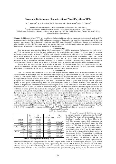
Stress and Performance Characteristics of Novel Polysilicon TFTs<br />
D. C. Moschou 1 , M. A. Exarchos 2 , D. N. Kouvatsos 1 , G. J. Papaioannou 2 and A. T. Voutsas 3<br />
1 Institute of Microelectronics, NCSR Demokritos, Agia Paraskevi 15310, Greece<br />
2 Physics Department, National and Kapodistrian University of Athens, Athens 15784, Greece<br />
3 LCD Process Technology Laboratory, Sharp Labs of America, 5700 NM Pacific Rim Blvd, Camas, WA 98607, USA<br />
*dmoschou@imel.demokritos.gr<br />
Abstract SLS ELA polysilicon TFTs fabricated in novel films of different microstructure and texture, were investigated. The<br />
parameter statistics indicate that the TFT performance depends on film quality and asperities, in conjunction with the grain<br />
boundary trap density. The drain current transients, upon TFT switch from OFF to ON state, showed oxide polarization,<br />
related to film asperities. DC hot carrier stress was applied, indicating a reliability dependence on polysilicon structure and<br />
differences in degradation mechanisms for various TFT technologies.<br />
1. Introduction<br />
Low temperature polycrystalline silicon thin film transistors (LTPS TFTs) are essential for large area electronic circuits<br />
and VLSI technology, as well as for high performance flat panel display applications [1]. Along with the increased<br />
performance characteristics of future LTPS TFTs, high reliability should also be achieved for the fabrication of commercial<br />
products to be possible. With the recent polysilicon crystallization process breakthroughs, using various excimer laser anneal<br />
(ELA) methods such as sequential lateral solidification (SLS), the TFT performance has substantially increased [2-4].<br />
Variations of the SLS technique allow the manufacturing of films with excellent intragrain quality and grains of different<br />
shapes and sizes. The performance and reliability of TFTs are known to depend on the polysilicon film microstructure [5].<br />
In this work we investigate the characteristics of top gate TFTs in polysilicon films, fabricated with various SLS<br />
crystallization methods, yielding different film textures and structures of grain boundaries. The device parameter statistics,<br />
the transient current behaviour and the TFT degradation under hot carrier stress are studied.<br />
2. Experimental<br />
The TFTs studied were fabricated in 50 nm thick polysilicon films, formed by ELA crystallization of a:Si, using<br />
variations of the SLS technique, with the laser beam being shaped by an appropriate mask. For our 2-shot samples the mask<br />
consists of two columns, slightly offset from each other, each with a set of parallel slits. This kind of polysilicon films has<br />
rectangular shaped crystal domains. A variation of this procedure is the 2 N -shot, where the laser beam is divided in a number<br />
of regions, with sets of slits, orthogonal to each other. This technique results in grains with excellent internal crystalline<br />
quality, as each spot is irradiated many times, and again rectangular grains. In this work, TFTs in 2 6 -shot films have been<br />
studied. In the procedure termed MN the mask consists again of sets of slits orthogonal to each other. The difference of this<br />
procedure with the 2 N -shot one is that in the latter technique one set of the slits irradiates the same region, and so does not<br />
contribute to lateral growth, but increases the intragrain quality. On the contrary, in the MN procedure all of the sets<br />
advance the lateral growth front, resulting in larger domain sizes of lower intragrain quality. There are also procedures where<br />
the beam shaping masks consist of arrays of dots, and so the lateral growth of the film begins from the dots and progresses<br />
radially, resulting in square or hexagonal shaped crystal domains separated by grain boundaries.<br />
The TFTs had a non-self-aligned top-metal-gate structure and a PECVD SiO2 gate dielectric. The TFTs and SIMOX<br />
MOSFETs, used as reference, were characterized and stressed using a HP4140B semiconductor analyzer. The I ds -V gs transfer<br />
characteristics were taken with V ds of 0.1 V, and the device parameters were extracted; furthermore, we applied Levinson<br />
analysis to calculate the grain-boundary trap densities of the TFTs. The drain current transients upon application of gate bias<br />
pulses, when unstressed TFTs are switched from OFF- to ON- state, were also investigated. A DC hot carrier stress (V gs , V ds )<br />
of (5 V, 10 V) was applied for a maximum of 16 hours, for TFTs fabricated in all of the above described samples.<br />
3. Results and Discussion<br />
A. Device characteristics<br />
V th<br />
(V)<br />
<br />
(cm 2 /Vsec)<br />
S<br />
(mV/decade)<br />
N t<br />
(cm -3 )<br />
SIMOX -0,57 322,15 0,11<br />
2-shot -1,87 282,31 0,39 6,57×10 11<br />
2 6 -shot 0,21 187,33 0,16 3,81×10 11<br />
Dot 30HEX -1,31 163,01 0,23 5,01×10 11<br />
50SQ 0,62 198,14 0,21 9,04×10 11<br />
MN #1 -1,03 235,40 0,17 3,4×10 11<br />
#7 -0,95 321,96 0,19 3,77×10 11<br />
#8 -0,20 289,08 0,15 3,03×10 11<br />
Table I: Device parameter average values<br />
From AFM images of the films, we observe<br />
an increased number of high protrusions for the 2 6 -<br />
shot film. The height of the protrusions becomes<br />
significantly smaller for the 2-shot film. In the<br />
MN film we again observe high protrusions, but<br />
much more sparsely distributed within the film<br />
surface. In Table I we can see the average values of<br />
the threshold voltage V th , the field-effect mobility<br />
, the subthreshold slope S and the grain-boundary<br />
trap density N t as obtained by Levinson analysis of<br />
the measured devices. We examined two different<br />
variations of the Dot technology and four of the<br />
MN technology, the differences, for the Dot<br />
technologies, being the hexagonal crystal domains<br />
for the 30Hex samples and the square ones for the 50Sq samples, while for the MN technologies being the crystal domain<br />
size. We can see that the largest mobility values, approaching the ones of SIMOX devices, are obtained for MN TFTs,<br />
followed closely by 2-shot and then by 2 6 -shot and Dot ones. This order of the different technologies with decreasing<br />
mobility can be attributed to the combination of two factors: the grain-boundary trap density N t and the surface asperities.<br />
74


