xxiii Ïανελληνιο ÏÏ Î½ÎµÎ´Ïιο ÏÏ ÏÎ¹ÎºÎ·Ï ÏÏεÏÎµÎ±Ï ÎºÎ±ÏαÏÏαÏÎ·Ï & εÏιÏÏÎ·Î¼Î·Ï ...
xxiii Ïανελληνιο ÏÏ Î½ÎµÎ´Ïιο ÏÏ ÏÎ¹ÎºÎ·Ï ÏÏεÏÎµÎ±Ï ÎºÎ±ÏαÏÏαÏÎ·Ï & εÏιÏÏÎ·Î¼Î·Ï ...
xxiii Ïανελληνιο ÏÏ Î½ÎµÎ´Ïιο ÏÏ ÏÎ¹ÎºÎ·Ï ÏÏεÏÎµÎ±Ï ÎºÎ±ÏαÏÏαÏÎ·Ï & εÏιÏÏÎ·Î¼Î·Ï ...

Create successful ePaper yourself
Turn your PDF publications into a flip-book with our unique Google optimized e-Paper software.
C/ C ox<br />
1,0<br />
0,8<br />
0,6<br />
0,4<br />
0,2<br />
0,0<br />
-4 -2 0 2 4<br />
V gate<br />
[V]<br />
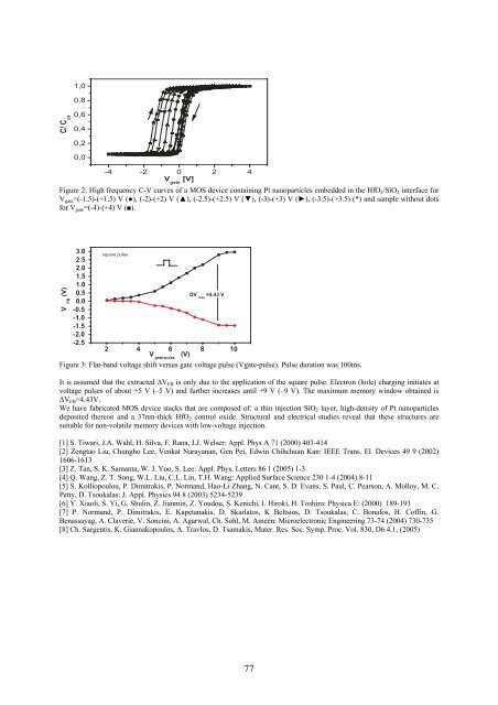
Figure 2: High frequency C-V curves of a MOS device containing Pt nanoparticles embedded in the HfO 2 /SiO 2 interface for<br />
V gate =(-1.5)-(+1.5) V (●), (-2)-(+2) V (▲), (-2.5)-(+2.5) V (▼), (-3)-(+3) V (►), (-3.5)-(+3.5) (*) and sample without dots<br />
for V gate =(-4)-(+4) V (■).<br />
V<br />
FB<br />
(V)<br />
3.0<br />
square pulse<br />
2.5<br />
2.0<br />
1.5<br />
1.0<br />
0.5<br />
DV max<br />
=4.43 V<br />
0.0<br />
-0.5<br />
-1.0<br />
-1.5<br />
-2.0<br />
-2.5<br />
2 4 6 8 10<br />
(V)<br />
V gate-pulse<br />
Figure 3: Flat-band voltage shift versus gate voltage pulse (Vgate-pulse). Pulse duration was 100ms.<br />
It is assumed that the extracted ΔV FB is only due to the application of the square pulse. Electron (hole) charging initiates at<br />
voltage pulses of about +5 V (–5 V) and further increases until +9 V (–9 V). The maximum memory window obtained is<br />
ΔV FB =4.43V.<br />
We have fabricated MOS device stacks that are composed of: a thin injection SiO 2 layer, high-density of Pt nanoparticles<br />
deposited thereon and a 37nm-thick HfO 2 control oxide. Structural and electrical studies reveal that these structures are<br />
suitable for non-volatile memory devices with low-voltage injection.<br />
[1] S. Tiwari, J.A. Wahl, H. Silva, F. Rana, J.J. Welser: Appl. Phys A 71 (2000) 403-414<br />
[2] Zengtao Liu, Chungho Lee, Venkat Narayanan, Gen Pei, Edwin Chihchuan Kan: IEEE Trans. El. Devices 49 9 (2002)<br />
1606-1613<br />
[3] Z. Tan, S. K. Samanta, W. J. Yoo, S. Lee: Appl. Phys. Letters 86 1 (2005) 1-3<br />
[4] Q. Wang, Z. T. Song, W.L. Liu, C.L. Lin, T.H. Wang: Applied Surface Science 230 1-4 (2004) 8-11<br />
[5] S. Kolliopoulou, P. Dimitrakis, P. Normand, Hao-Li Zhang, N. Cant, S. D. Evans, S. Paul, C. Pearson, A. Molloy, M. C.<br />
Petty, D. Tsoukalas: J. Appl. Physics 94 8 (2003) 5234-5239<br />
[6] Y. Xiaoli, S. Yi, G. Shulin, Z. Jianmin, Z. Youdou, S. Kenichi, I. Hiroki, H. Toshiro: Physica E: (2000) 189-193<br />
[7] P. Normand, P. Dimitrakis, E. Kapetanakis, D. Skarlatos, K Beltsios, D. Tsoukalas, C. Bonafos, H. Coffin, G.<br />
Benassayag, A. Claverie, V. Soncini, A. Agarwal, Ch. Sohl, M. Ameen: Microelectronic Engineering 73-74 (2004) 730-735<br />
[8] Ch. Sargentis, K. Giannakopoulos, A. Travlos, D. Tsamakis, Mater. Res. Soc. Symp. Proc. Vol. 830, D6.4.1, (2005)<br />
77