xxiii Ïανελληνιο ÏÏ Î½ÎµÎ´Ïιο ÏÏ ÏÎ¹ÎºÎ·Ï ÏÏεÏÎµÎ±Ï ÎºÎ±ÏαÏÏαÏÎ·Ï & εÏιÏÏÎ·Î¼Î·Ï ...
xxiii Ïανελληνιο ÏÏ Î½ÎµÎ´Ïιο ÏÏ ÏÎ¹ÎºÎ·Ï ÏÏεÏÎµÎ±Ï ÎºÎ±ÏαÏÏαÏÎ·Ï & εÏιÏÏÎ·Î¼Î·Ï ...
xxiii Ïανελληνιο ÏÏ Î½ÎµÎ´Ïιο ÏÏ ÏÎ¹ÎºÎ·Ï ÏÏεÏÎµÎ±Ï ÎºÎ±ÏαÏÏαÏÎ·Ï & εÏιÏÏÎ·Î¼Î·Ï ...

You also want an ePaper? Increase the reach of your titles
YUMPU automatically turns print PDFs into web optimized ePapers that Google loves.
Fabrication of a MOS Memory Device Containing Metal Nanoparticles and a high-k<br />
Control Oxide Layer<br />
Ch. Sargentis 1* , K. Giannakopoulos 2 , A. Travlos 2 and D. Tsamakis 1<br />
1 Department of Electrical and Computer Engineering, National Technical University of Athens, Iroon Polytechniou 9<br />
Zografou,157 73 Athens, Greece<br />
2 Institute of Materials Science, National Center for Scientific Research `Demokritos`, 153 10 Ag. Paraskevi Attikis, Athens,<br />
Greece<br />
*sargent@central.ntua.gr<br />
Today many electronic devices, such as laptops, palmtops, cellular phones and digital cameras use non-volatile memories<br />
that have a very short access time, low power consumption, high memory density and long retention times. Most efforts on<br />
improving these devices are focused on the developement of MOSFET floating gate devices embedded with semiconductor<br />
nanoparticles [1-7]. Recently, similar devices, embedded with metallic nanoparticles, have been fabricated [2-5]. These<br />
devices [2] are relatively immune to the Fermi level fluctuations caused by contamination and have smaller energy<br />
perturbation than those based on semiconductor nanoparticles. Since metals can have a wide range of work functions, it is<br />
possible to use them for improving the relationship between the retention time and the speed of the write-erase process,<br />
parameters that one needs to balance during device design. Memory devices embedded with nanoparticles have been<br />
fabricated with various methods, such as: Chemical Vapor Deposition [6], ion beam synthesis [7], sputtering [3] and recently<br />
Molecular Beam Epitaxy (MBE) [4]. In this work we use the MBE method in order to fabricate MOS memory structures<br />
embedded with platinum (Pt) nanoparticles on a SiO 2 /HfO 2 interface. We have chosen to work with Pt nanoparticles due to<br />
the fact that Pt has a large work function.<br />
Initially we grew thermally a 3.5 nm dry SiO 2 layer (tunneling oxide) on a n-Si (001) substrate. This oxide layer is fabricated<br />
in a furnace with dry thermal oxidation at 850 ºC. We have chosen such a low temperature in order to have good thickness<br />
control. Immediately after, the sample is annealed at 920 ºC in nitrogen ambient for 20 minutes in order to remove any states<br />
in the SiO 2 layer. Then, 1 nm of Pt is deposited at room temperature; the Pt is evaporated with the use of an electron gun in<br />
the MBE system. Next, 37 nm of a HfO 2 control oxide layer are deposited at 200 º C in an oxygen rich ambient, so that it<br />
becomes as stoichiometric as possible.<br />
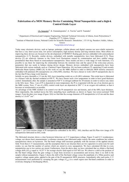
An advantage of the MBE method is its control over the Pt nanoparticle size and density, and of the HfO 2 layer thickness.<br />
Most importantly, this method leaves the SiO 2 tunnelling layer unaffected, as shown in Figure 1(a) (cross-sectional TEM<br />
image). From the plan view image (Figure 1(b)) we find that the average diameter of Pt nanoparticles is 4,9 nm and the sheet<br />
density is 3.2x10 12 cm -2 .<br />
Figure 1: (a) Cross-section image of Pt nanoparticles embedded in the HfO 2 / SiO 2 interface and (b) Plan-view image of Pt<br />
nanoparticles fabricated on SiO 2 oxide<br />
The fabricated structure shows a clear hysteresis behaviour on C-V (capacitance-voltage, Figure 2) and G-V (conductancevoltage,<br />
not shown here) measurements; a reference structure (one fabricated under exactly the same conditions but without<br />
nanoparticles) shows no hysteresis. The flat band voltage shift increases gradually with the increase of the applied electric<br />
field. From these C-V measurements, and the assumption that in our structure there are two capacitors in series (one for each<br />
oxide), we can find the number of carriers which are stored in every nanoparticle. We have calculated [8] that in every<br />
nanoparticles one to two carriers are stored. Furthermore, from the above data, we have calculated that we obtain a flat-band<br />
voltage shift (ΔV FB ) equal to +0.257 V for average electric field equal to 0.65 MV/cm. We observe a shift at the position of<br />
the flat band voltage when the gate voltage is swept from inversion to accumulation and inverse; there is no shift in the<br />
sample without nanoparticles. Figure 3 shows the shift of the flat-band voltage versus the amplitude of a 100ms positive and<br />
negative voltage square pulse, applied to the gate of the Pt nanoparticle MOS structures. Immediately after each pulse, C-V<br />
measurements were performed by sweeping the gate voltage (V gate ) in a small region near flat-band conditions in order to<br />
avoid any charging or discharging effects.<br />
76