xxiii Ïανελληνιο ÏÏ Î½ÎµÎ´Ïιο ÏÏ ÏÎ¹ÎºÎ·Ï ÏÏεÏÎµÎ±Ï ÎºÎ±ÏαÏÏαÏÎ·Ï & εÏιÏÏÎ·Î¼Î·Ï ...
xxiii Ïανελληνιο ÏÏ Î½ÎµÎ´Ïιο ÏÏ ÏÎ¹ÎºÎ·Ï ÏÏεÏÎµÎ±Ï ÎºÎ±ÏαÏÏαÏÎ·Ï & εÏιÏÏÎ·Î¼Î·Ï ...
xxiii Ïανελληνιο ÏÏ Î½ÎµÎ´Ïιο ÏÏ ÏÎ¹ÎºÎ·Ï ÏÏεÏÎµÎ±Ï ÎºÎ±ÏαÏÏαÏÎ·Ï & εÏιÏÏÎ·Î¼Î·Ï ...

You also want an ePaper? Increase the reach of your titles
YUMPU automatically turns print PDFs into web optimized ePapers that Google loves.
V th<br />
(V)<br />
G m,max<br />
/G m,max0<br />
(%)<br />
I d<br />
(mA)<br />
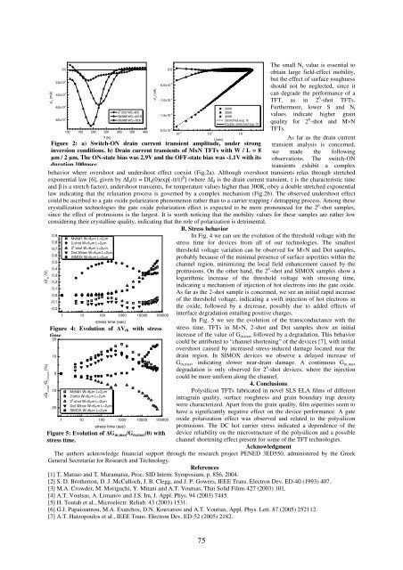
Figure 2: a) Switch-ON drain current transient amplitude, under strong<br />
inversion conditions. b) Drain current transients of MxN TFTs with W / L = 8<br />
m / 2 m. The -state bias was 2.9V and the OFF-state bias was -1.1V with its<br />
The small N t value is essential to<br />
obtain large field-effect mobility,<br />
but the effect of surface roughness<br />
should not be neglected, since it<br />
can degrade the performance of a<br />
TFT, as in 2 6 -shot TFTs.<br />
Furthermore, lower S and N t<br />
values indicate higher grain<br />
quality for 2 6 -shot and MN<br />
TFTs.<br />
As far as the drain current<br />
transient analysis is concerned,<br />
we made the following<br />
observations. The switch-ON<br />
transients exhibit a complex<br />
duration 100msec.<br />
behavior where overshoot and undershoot effect coexist (Fig.2a). Although overshoot transients relax through stretched<br />
exponential law [6], given by I d (t) = D d (0)exp[-(t/) ] (where I d is the drain current transient, is the characteristic time<br />
and is a stretch factor), undershoot transients, for temperature values higher than 300K, obey a double stretched exponential<br />
law indicating that the relaxation process is governed by a complex mechanism (Fig.2b). The observed undershoot effect<br />
could be ascribed to a gate oxide polarization phenomenon rather than to a carrier trapping / detrapping process. Among these<br />
crystallization technologies the gate oxide polarization effect is expected to be more pronounced for the 2 6 -shot samples,<br />
since the effect of protrusions is the largest. It is worth noticing that the mobility values for these samples are rather low<br />
considering their crystalline quality, indicating that the role of polarization is detrimental.<br />
B. Stress behavior<br />
0,9<br />
0,8<br />
0,7<br />
0,6<br />
0,5<br />
0,4<br />
0,3<br />
0,2<br />
0,1<br />
0,0<br />
-0,1<br />
-0,2<br />
20<br />
10<br />
0<br />
-10<br />
-20<br />
0,0<br />
-2,0x10 -4<br />
-4,0x10 -4<br />
-6,0x10 -4<br />
-8,0x10 -4<br />
100 150 200 250 300 350 400<br />
T (K)<br />
MxN#1 W=8m L=2m<br />
2-shot W=8m L=2m<br />
2 6 -shot W=8m L=2m<br />
Dot 30hex W=6m L=2m<br />
SIMOX W=8m L=2m<br />
1 10 100 1000 10000 100000<br />
stress time (sec)<br />
MxN#1 W=8m L=2m<br />
2-shot W=8m L=2m<br />
2 6 -shot W=8m L=2m<br />
Dot 30hex W=6m L=2m<br />
SIMOX W=8m L=2m<br />
2 6 -shot W/L=8/5<br />
MxN#8 W/L=4/0.8<br />
MxN#8 W/L=16/8<br />
Figure 4: Evolution of V th with stress<br />
time.<br />
1 10 100 1000 10000 100000<br />
stress time (sec)<br />
Figure 5: Evolution of G m,max /G m,max (0) with<br />
stress time.<br />
I d (mA)<br />
0,0<br />
-5,0x10 -5<br />
-1,0x10 -4<br />
-1,5x10 -4<br />
-2,0x10 -4<br />
200K<br />
300K<br />
400K<br />
Stretched exp. fit<br />
Double stretched exp. fit<br />
10 -3 10 -2 10 -1<br />
In Fig. 4 we can see the evolution of the threshold voltage with the<br />
stress time for devices from all of our technologies. The smallest<br />
threshold voltage variation can be observed for MN and Dot samples,<br />
probably because of the minimal presence of surface asperities within the<br />
channel region, minimizing the local field enhancement caused by the<br />
protrusions. On the other hand, the 2 6 -shot and SIMOX samples show a<br />
logarithmic increase of the threshold voltage with stressing time,<br />
indicating a mechanism of injection of hot electrons into the gate oxide.<br />
As far as the 2-shot sample is concerned, we see an initial rapid increase<br />
of the threshold voltage, indicating a swift injection of hot electrons in<br />
the oxide, followed by a decrease, possibly due to added effects of<br />
interface degradation entailing positive charges.<br />
In Fig. 5 we see the evolution of the transconductance with the<br />
stress time. TFTs in MN, 2-shot and Dot samples show an initial<br />
increase of the value of G m,max followed by a degradation. This behavior<br />
could be attributed to “channel shortening” of the devices [7], with initial<br />
overshoot caused by increased stress-induced damage located near the<br />
drain region. In SIMOX devices we observe a delayed increase of<br />
G m,max , indicating slower near-drain damage. A continuous G m,max<br />
degradation is only observed for 2 6 -shot devices, where the injection<br />
could be more uniform along the channel.<br />
4. Conclusions<br />
Polysilicon TFTs fabricated in novel SLS ELA films of different<br />
intragrain quality, surface roughness and grain boundary trap density<br />
were characterized. Apart from the grain quality, film asperities seem to<br />
have a significantly negative effect on the device performance. A gate<br />
oxide polarization effect was observed and related to the polysilicon<br />
protrusions. The DC hot carrier stress indicated a dependence of the<br />
device reliability on the microstructure of the polysilicon and a possible<br />
channel shortening effect present for some of the TFT technologies.<br />
Acknowledgment<br />
The authors acknowledge financial support through the research project PENED 3ED550, administered by the Greek<br />
General Secretariat for Research and Technology.<br />
References<br />
[1] T. Matsuo and T. Muramatsu, Proc. SID Intern. Symposium, p. 856, 2004.<br />
[2] S. D. Brotherton, D. J. McCulloch, J. B. Clegg, and J. P. Gowers, IEEE Trans. Electron Dev. ED-40 (1993) 407.<br />
[3] M.A. Crowder, M. Moriguchi, Y. Mitani and A.T. Voutsas, Thin Solid Films 427 (2003) 101.<br />
[4] A.T. Voutsas, A. Limanov and J.S. Im, J. Appl. Phys. 94 (2003) 7445.<br />
[5] H. Toutah et al., Microelectr. Reliab. 43 (2003) 1531.<br />
[6] G.J. Papaioannou, M.A. Exarchos, D.N. Kouvatsos and A.T. Voutsas, Appl. Phys. Lett. 87 (2005) 252112.<br />
[7] A.T. Hatzopoulos et al., IEEE Trans. Electron Dev. ED-52 (2005) 2182.<br />
t (sec)<br />
75