xxiii Ïανελληνιο ÏÏ Î½ÎµÎ´Ïιο ÏÏ ÏÎ¹ÎºÎ·Ï ÏÏεÏÎµÎ±Ï ÎºÎ±ÏαÏÏαÏÎ·Ï & εÏιÏÏÎ·Î¼Î·Ï ...
xxiii Ïανελληνιο ÏÏ Î½ÎµÎ´Ïιο ÏÏ ÏÎ¹ÎºÎ·Ï ÏÏεÏÎµÎ±Ï ÎºÎ±ÏαÏÏαÏÎ·Ï & εÏιÏÏÎ·Î¼Î·Ï ...
xxiii Ïανελληνιο ÏÏ Î½ÎµÎ´Ïιο ÏÏ ÏÎ¹ÎºÎ·Ï ÏÏεÏÎµÎ±Ï ÎºÎ±ÏαÏÏαÏÎ·Ï & εÏιÏÏÎ·Î¼Î·Ï ...

Create successful ePaper yourself
Turn your PDF publications into a flip-book with our unique Google optimized e-Paper software.
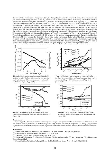
forwarded to the back interface during stress. Thus, the damaged region is located at the back drain-polysilicon interface. As<br />
hot-hole induced damage becomes severe, V th increases due to the induced interface state density. At the front interface<br />
possibly hot-electrons damage the polysilicon/SiO 2 interface and/or the grain boundaries, thus degrading G m,max . When the<br />
device was subjected to a stress condition with V GB,stress = 3 V, V th decreased for V GB = - 3 V and increased for V GB = 3 V.<br />
Moreover, G m,max degradation is larger than for previous stress conditions. Since, for V GB,stress >0, the vertical electric field is<br />
enhanced, it promotes hot-hole injection at the front interface, while hot electrons are accelerated towards the back interface.<br />
Indeed, under this condition hot-holes and hot-electrons acquire more energy to be directly injected in the front- and in the<br />
BG oxide respectively. As a result, hot-hole induced interface state generation is enhanced at the front interface and electron<br />
injection at the BG oxide provokes an additional negative V th shift, when measured at V GB = - 3 V. In the case of V GB,stress = 0<br />
V, V th is decreased by the same amount for all BG voltages. In this case, the V th decrease appears in the subthreshold region.<br />
This is possible if we consider that the positive charge in the back oxide increases during aging. Therefore, it is suggested that<br />
moderate hot-hole injection occurs in the BG oxide with no observable interface state generation phenomena. Regarding the<br />
front interface degradation, since the G m,max variation is identical to that for the stress condition V GB,stress = - 3 V, we propose<br />
that the observed degradation arises from hot-electron damage at the poly/SiO 2 interface and/or grain boundaries.<br />
Maximum transconductance, G m,max<br />
[A/V]<br />
1.3x10 -5<br />
1.2x10 -5<br />
2<br />
1.1x10 -5<br />
1.0x10 -5<br />
0<br />
9.0x10 -6<br />
8.0x10 -6<br />
-2<br />
7.0x10 -6<br />
-3 -2 -1 0 1 2 3<br />
Back gate voltage, V GB<br />
[V]<br />
Figure 1: Maximum transconductance and threshold<br />
voltage variation for front gate operation as a function<br />
back-gate biasing. All measurements are performed<br />
in the linear regime (V DS =0.1 V).<br />
Threshold voltage, V th<br />
[V]<br />
-(G m,max<br />
/G m,0<br />
)/G m,0<br />
(%)<br />
50 V GB,stress<br />
= -3 V<br />
40<br />
V GB,stress<br />
= 0 V<br />
V GB,stress<br />
= 3 V<br />
30<br />
20<br />
10<br />
0<br />
10 0 10 1 10 2 10 3 10 4<br />
Stress time [s]<br />
Figure 2: Maximum transconductance variation (%) for<br />
the three stress conditions (differing back-gate stress bias) of<br />
measured at V GB = - 3 V (filled marks) and V GB = 3 V<br />
(open marks).<br />
∆V th<br />
[V]<br />
0.0<br />
-0.1<br />
-0.2<br />
-0.3<br />
-0.4<br />
-0.5<br />
-0.6<br />
V GB,stress<br />
= -3 V<br />
V GB,stress<br />
= 0 V<br />
V GB,stress<br />
= 3 V<br />
measured at<br />
V GB<br />
= -3 V<br />
10 0 10 1 10 2 10 3 10 4<br />
Stress time [s]<br />
∆V th<br />
[V]<br />
1.5<br />
1.2<br />
0.9<br />
0.6<br />
0.3<br />
0.0<br />
-0.3<br />
-0.6<br />
-0.9<br />
V GB,stress<br />
= -3 V<br />
V GB,stress<br />
= 0 V<br />
V GB,stress<br />
= 3 V<br />
measured at<br />
V GB<br />
= +3 V<br />
10 0 10 1 10 2 10 3 10 4<br />
Stress time [s]<br />
Figure 3: Threshold voltage shift for the three stress<br />
Figure 4: Threshold voltage shift for the three stress<br />
conditions (differing back-gate stress bias) measured at<br />
conditions (differing back-gate stress bias) measured at<br />
V GB =- 3 V. V GB = 3 V.<br />
Conclusions<br />
It was suggested that stress conditions with negative back-gate voltage enhance hot-hole injection in the BG oxide and<br />
hot-electron induced phenomena at the front polysilicon/SiO 2 interface. In contrast, for positive BG during aging, hot-hole<br />
injection at the front interface revealed serious degradation with combined hot-electron induced effects at the back interface.<br />
References<br />
[1] Farmakis FV, Brini J, Kamarinos G and Dimitriadis CA. IEEE Electron Dev. Lett. 22 (2001) 74.<br />
[2] Cristoloveanu S. Microelectronics Reliability, 37, (1997), 1003.<br />
[3] Voutsas AT. IEEE Trans. Electron Devices 50 (2003) 1494.<br />
[4] Farmakis FV, Kouvatsos DN, Voutsas AT, Moschou DC, Kontogiannopoulos GP, and Papaioannou GJ. J. Electrochem.<br />
Soc. to be published.<br />
[5] Banna SR, Chan PCH, Chan M, Fung SKH and Ko PK. IEEE Trans. Electr. Dev., vol. 45, (1998), 206-212.<br />
71