- Page 1 and 2:
Intel ® 865G/865GV ChipsetDatashee
- Page 3:
Contents1 Introduction.............
- Page 6 and 7:
3.8 PCI-to-CSA Bridge Registers (De
- Page 8 and 9:
5.5.3 Synchronous Display .........
- Page 10 and 11:
Tables1 General Terminology .......
- Page 14:
This page is intentionally left bla
- Page 20 and 21:
Introduction1.4 Intel ® 82865G GMC
- Page 24:
Introduction1.4.7 Display Interface
- Page 27 and 28:
Signal Description2.1 Host Interfac
- Page 29 and 30:
Signal DescriptionSignal Name Type
- Page 31 and 32:
Signal Description2.2.2 DDR SDRAM C
- Page 33 and 34:
Signal Description2.5 AGP Interface
- Page 35 and 36:
Signal Description2.5.4 AGP Strobes
- Page 37 and 38:
Signal DescriptionSignal Name Type
- Page 39 and 40:
Signal Description2.5.7 Intel ® DV
- Page 41 and 42:
Signal Description2.7 Clocks, Reset
- Page 44 and 45:
Signal Description2.10 GMCH Sequenc
- Page 46 and 47:
Signal Description2.12 Full and War
- Page 48 and 49:
Register DescriptionTermReservedReg
- Page 50 and 51:
Register Description3.3 Routing Con
- Page 52 and 53:
Register DescriptionIf the Bus Numb
- Page 54 and 55:
Register Description3.4.2 CONFIG_DA
- Page 56 and 57:
Register DescriptionTable 6.DRAM Co
- Page 58 and 59:
Register Description3.5.3 PCICMD—
- Page 60 and 61:
Register Description3.5.5 RID—Rev
- Page 62 and 63:
Register Description3.5.10 APBASE
- Page 64 and 65:
Register Description3.5.14 AGPM—A
- Page 66 and 67:
Register DescriptionNotes on Pre-Al
- Page 68 and 69:
Register Description3.5.17 FPLLCONT
- Page 70 and 71:
Register DescriptionAs an example,
- Page 72 and 73:
Register Description3.5.20 SMRAM—
- Page 74 and 75:
Register Description3.5.22 ACAPID
- Page 76 and 77:
Register Description3.5.24 AGPCMD
- Page 78 and 79:
Register Description3.5.26 APSIZE
- Page 80 and 81:
Register Description3.5.29 LPTT—A
- Page 82 and 83: Register Description3.5.31 GMCHCFG
- Page 84 and 85: Register Description3.5.32 ERRSTS
- Page 86 and 87: Register Description3.5.34 SKPD—S
- Page 88 and 89: Register Description3.6.1 VID1—Ve
- Page 90 and 91: Register Description3.6.4 PCISTS1
- Page 92 and 93: Register Description3.6.8 MLT1—Ma
- Page 94 and 95: Register Description3.6.14 IOBASE1
- Page 96 and 97: Register Description3.6.17 MBASE1
- Page 100: Register Description3.6.22 ERRCMD1
- Page 105 and 106: Register Description3.7.6 CC—Clas
- Page 107 and 108: Register Description3.7.11 MMADR—
- Page 109 and 110: Register Description3.7.16 CAPPOINT
- Page 111 and 112: Register Description3.7.22 PMCAP—
- Page 113 and 114: Register Description3.8 PCI-to-CSA
- Page 115 and 116: Register Description3.8.3 PCICMD3
- Page 117 and 118: Register Description3.8.5 RID3—Re
- Page 119 and 120: Register Description3.8.11 SBUSN3
- Page 121 and 122: Register Description3.8.15 SSTS3—
- Page 123 and 124: Register Description3.8.17 MLIMIT3
- Page 125 and 126: Register Description3.8.20 BCTRL3
- Page 127 and 128: Register Description3.9 Overflow Co
- Page 129 and 130: Register Description3.9.4 PCISTS6
- Page 131: Register Description3.9.9 BAR6—Me
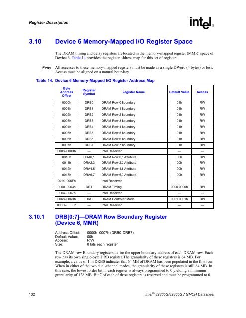
- Page 135 and 136: Register Description3.10.3 DRT—DR
- Page 137 and 138: Register DescriptionBit6:4Descripti
- Page 139 and 140: System Address MapSystem Address Ma
- Page 141 and 142: System Address Map4.2 Compatibility
- Page 143 and 144: System Address Map4.3 Extended Memo
- Page 145 and 146: System Address MapPCI Memory Addres
- Page 147 and 148: Functional DescriptionFunctional De
- Page 149 and 150: Functional Description5.2 System Me
- Page 151 and 152: Functional Description5.2.2.1 Dynam
- Page 153 and 154: Functional DescriptionTable 21. DRA
- Page 155 and 156: Functional DescriptionTable 23. DRA
- Page 157 and 158: Functional Description5.2.6 Configu
- Page 159 and 160: Functional Description5.3.1 GMCH AG
- Page 161 and 162: Functional Descriptiondown controll
- Page 163 and 164: Functional Description5.3.6 Support
- Page 165 and 166: Functional Description5.4.1 3D Engi
- Page 167 and 168: Functional DescriptionTexture Forma
- Page 169 and 170: Functional DescriptionTexture Map B
- Page 171 and 172: Functional DescriptionDepth BufferT
- Page 173 and 174: Functional Description5.4.3 Video E
- Page 175 and 176: Functional Description5.4.5 PipesSc
- Page 177 and 178: Functional DescriptionIntegrated RA
- Page 179 and 180: Functional DescriptionDirect YUV fr
- Page 181 and 182: Functional Description• System—
- Page 183 and 184:
Functional Description5.8 ClockingT
- Page 185 and 186:
Electrical CharacteristicsElectrica
- Page 187 and 188:
Electrical CharacteristicsTable 36.
- Page 189 and 190:
Electrical Characteristics6.5 DC Pa
- Page 191 and 192:
Electrical CharacteristicsTable 38.
- Page 193 and 194:
Electrical CharacteristicsTable 38.
- Page 195 and 196:
Electrical Characteristics6.6.3 DAC
- Page 197 and 198:
Ballout and Package InformationBall
- Page 199 and 200:
Ballout and Package InformationFigu
- Page 201 and 202:
Ballout and Package InformationTabl
- Page 203 and 204:
Ballout and Package InformationTabl
- Page 205 and 206:
Ballout and Package InformationTabl
- Page 207 and 208:
Ballout and Package InformationTabl
- Page 209 and 210:
Ballout and Package Information7.2
- Page 211 and 212:
TestabilityTestability 8In the GMCH
- Page 213 and 214:
Testability8.2 XOR Chain Definition
- Page 215 and 216:
TestabilityTable 45. XOR Chain 1 (3
- Page 217 and 218:
TestabilityTable 49. XOR Chain 5 (4
- Page 219 and 220:
TestabilityTable 53. XOR Chain 9 (6
- Page 221 and 222:
Intel ® 82865GV GMCHIntel ® 82865
- Page 223 and 224:
Intel ® 82865GV GMCH9.3 Intel ® 8
- Page 225 and 226:
Intel ® 82865GV GMCHGMCHCFG—GMCH
- Page 227 and 228:
Intel ® 82865GV GMCH BalloutIntel
- Page 229 and 230:
Intel ® 82865GV GMCH BalloutFigure
- Page 231 and 232:
Intel ® 82865GV GMCH BalloutTable
- Page 233 and 234:
Intel ® 82865GV GMCH BalloutTable
- Page 235 and 236:
Intel ® 82865GV GMCH BalloutTable
- Page 237 and 238:
Intel ® 82865GV GMCH BalloutTable
- Page 239 and 240:
Intel ® 82865GV GMCH BalloutTable
- Page 241 and 242:
Intel ® 82865GV GMCH TestabilityIn
- Page 243 and 244:
Intel ® 82865GV GMCH Testability11
- Page 245 and 246:
Intel ® 82865GV GMCH TestabilityTa
- Page 247 and 248:
Intel ® 82865GV GMCH TestabilityTa
- Page 249 and 250:
Intel ® 82865GV GMCH TestabilityTa