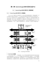
Intel® 865G/865GV Chipset Datasheet - download.intel.nl - Intel
Intel® 865G/865GV Chipset Datasheet - download.intel.nl - Intel
Intel® 865G/865GV Chipset Datasheet - download.intel.nl - Intel

Create successful ePaper yourself
Turn your PDF publications into a flip-book with our unique Google optimized e-Paper software.
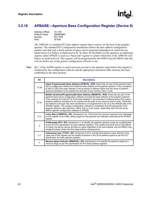
Register Description3.5.10 APBASE—Aperture Base Configuration Register (Device 0)Address Offset: 10–13hDefault Value: 00000008hAccess:RO, R/WSize:32 bitsThe APBASE is a standard PCI base address register that is used to set the base of the graphicsaperture. The standard PCI Configuration mechanism defines the base address configurationregister such that o<strong>nl</strong>y a fixed amount of space can be requested (dependent on which bits arehardwired to 0 or behave as hardwired to 0). To allow for flexibility (of the aperture) an additionalregister called APSIZE is used as a “back-end” register to control which bits of the APBASE willbehave as hardwired to 0. This register will be programmed by the GMCH specific BIOS code thatwill run before any of the generic configuration software is run.Note:Bit 1 of the AGPM register is used to prevent accesses to the aperture range before this register isinitialized by the configuration software and the appropriate translation table structure has beenestablished in the main memory.Bit31:2827:2221:432:10DescriptionsUpper Programmable Base Address (UPBITS)—R/W. These bits are part of the aperture baseset by configuration software to locate the base address of the graphics aperture. They correspondto bits [31:28] of the base address in the processor's address space that will cause a graphicsaperture translation to be inserted into the path of any memory read or write.Middle Hardwired/Programmable Base Address (MIDBITS)—R/W. These bits are part of theaperture base set by configuration software to locate the base address of the graphics aperture.They correspond to bits [27:4] of the base address in the processor's address space that cause agraphics aperture translation to be inserted into the path of any memory read or write. These bitscan behave as though they were hardwired to 0 if programmed to do so by the APSIZE bits of theAPSIZE register. This causes configuration software to understand that the granularity of thegraphics aperture base address is either finer or more coarse, depending upon the bits set byGMCH-specific configuration software in APSIZE.Lower Bits (LOWBITS)—RO. Hardwired to 0s. This forces the minimum aperture size selectableby this register to be 4 MB, without regard to the aperture size definition enforced by the APSIZEregister.Prefetchable (PF)—RO. Hardwired to 1 to identify the graphics aperture range as a prefetchableas per the PCI specification for base address registers. This implies that there are no side effectson reads, the device returns all bytes on reads regardless of the byte enables, and the GMCH maymerge processor writes into this range without causing errors.Addressing Type (TYPE)—RO. Hardwired to 00 to indicate that address range defined by theupper bits of this register can be located anywhere in the 32-bit address space as per the PCIspecification for base address registers.Memory Space Indicator (MSPACE)—RO. Hardwired to 0 to identify the aperture range as amemory range as per the specification for PCI base address registers.62 <strong>Intel</strong> ® 82<strong>865G</strong>/82<strong>865G</strong>V GMCH <strong>Datasheet</strong>