Intel® 865G/865GV Chipset Datasheet - download.intel.nl - Intel
Intel® 865G/865GV Chipset Datasheet - download.intel.nl - Intel
Intel® 865G/865GV Chipset Datasheet - download.intel.nl - Intel

Create successful ePaper yourself
Turn your PDF publications into a flip-book with our unique Google optimized e-Paper software.
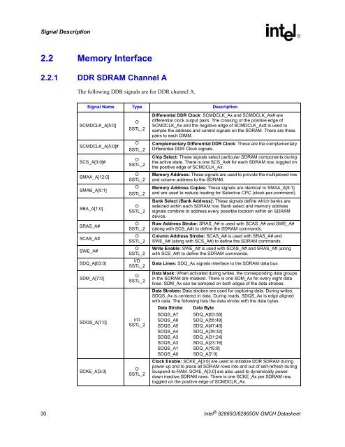
Signal Description2.2 Memory Interface2.2.1 DDR SDRAM Channel AThe following DDR signals are for DDR channel A.Signal Name Type DescriptionSCMDCLK_A[5:0]SCMDCLK_A[5:0]#SCS_A[3:0]#SMAA_A[12:0]SMAB_A[5:1]SBA_A[1:0]SRAS_A#SCAS_A#SWE_A#SDQ_A[63:0]SDM_A[7:0]SDQS_A[7:0]SCKE_A[3:0]OSSTL_2OSSTL_2OSSTL_2OSSTL_2OSSTL_2OSSTL_2OSSTL_2OSSTL_2OSSTL_2I/OSSTL_2OSSTL_2I/OSSTL_2OSSTL_2Differential DDR Clock: SCMDCLK_Ax and SCMDCLK_Ax# aredifferential clock output pairs. The crossing of the positive edge ofSCMDCLK_Ax and the negative edge of SCMDCLK_Ax# is used tosample the address and control signals on the SDRAM. There are threepairs to each DIMM.Complementary Differential DDR Clock: These are the complementaryDifferential DDR Clock signals.Chip Select: These signals select particular SDRAM components duringthe active state. There is one SCS_Ax# for each SDRAM row, toggled onthe positive edge of SCMDCLK_Ax.Memory Address: These signals are used to provide the multiplexed rowand column address to the SDRAM.Memory Address Copies: These signals are identical to SMAA_A[5:1]and are used to reduce loading for Selective CPC (clock-per-command).Bank Select (Bank Address): These signals define which banks areselected within each SDRAM row. Bank select and memory addresssignals combine to address every possible location within an SDRAMdevice.Row Address Strobe: SRAS_A# is used with SCAS_A# and SWE_A#(along with SCS_A#) to define the SDRAM commands.Column Address Strobe: SCAS_A# is used with SRAS_A# andSWE_A# (along with SCS_A#) to define the SDRAM commands.Write Enable: SWE_A# is used with SCAS_A# and SRAS_A# (alongwith SCS_A#) to define the SDRAM commands.Data Lines: SDQ_Ax signals interface to the SDRAM data bus.Data Mask: When activated during writes, the corresponding data groupsin the SDRAM are masked. There is one SDM_Ax for every eight datalines. SDM_Ax can be sampled on both edges of the data strobes.Data Strobes: Data strobes are used for capturing data. During writes,SDQS_Ax is centered in data. During reads, SDQS_Ax is edge alignedwith data. The following lists the data strobe with the data bytes.Data Strobe Data ByteSDQS_A7 SDQ_A[63:56]SDQS_A6 SDQ_A[55:48]SDQS_A5 SDQ_A[47:40]SDQS_A4 SDQ_A[39:32]SDQS_A3 SDQ_A[31:24]SDQS_A2 SDQ_A[23:16]SDQS_A1 SDQ_A[15:8]SDQS_A0 SDQ_A[7:0]Clock Enable: SCKE_A[3:0] are used to initialize DDR SDRAM duringpower-up and to place all SDRAM rows into and out of self-refresh duringSuspend-to-RAM. SCKE_A[3:0] are also used to dynamically powerdown inactive SDRAM rows. There is one SCKE_Ax per SDRAM row,toggled on the positive edge of SCMDCLK_Ax.30 <strong>Intel</strong> ® 82<strong>865G</strong>/82<strong>865G</strong>V GMCH <strong>Datasheet</strong>