

Xilinx UG194 Virtex-5 FPGA Embedded Tri-Mode Ethernet MAC ...
Xilinx UG194 Virtex-5 FPGA Embedded Tri-Mode Ethernet MAC ...
Xilinx UG194 Virtex-5 FPGA Embedded Tri-Mode Ethernet MAC ...

Create successful ePaper yourself
Turn your PDF publications into a flip-book with our unique Google optimized e-Paper software.
Chapter 4: Host/DCR Bus Interfaces<br />
The register definitions for the DCR bridge registers are shown in Table 4-16 to Table 4-19.<br />
The DCR registers (dataRegMSW, dataRegLSW, cntlReg, and RDYstatus_e#) and the DCR<br />
bridge registers (IRSTATUS_e#, IRENABLE_e#, and MIIMWRDATA) use the big-endian<br />
bit numbering convention. The <strong>Ethernet</strong> <strong>MAC</strong> host registers, such as Receiver<br />
Configuration (Word 0) (host address 0x200) register, use the little-endian bit numbering<br />
convention. In the DCR bridge implementation, there is no conversion to or from big<br />
endian to little endian. The bit positions are mapped directly in a one-to-one<br />
correspondence (big-endian bit [0] is mapped directly to little-endian bit [31], bit [1] is<br />
mapped directly to little endian bit [30], and so forth).<br />
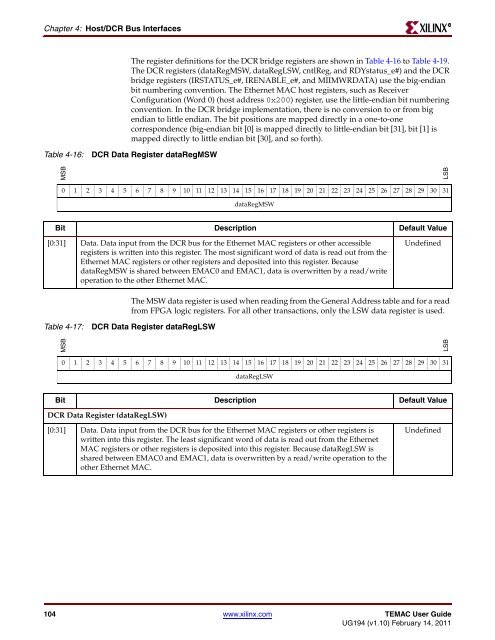
Table 4-16: DCR Data Register dataRegMSW<br />
MSB<br />
0 1 2 3 4 5 6 7 8 9 10 11 12 13 14 15 16 17 18 19 20 21 22 23 24 25 26 27 28 29 30 31<br />
dataRegMSW<br />
Bit Description Default Value<br />
[0:31] Data. Data input from the DCR bus for the <strong>Ethernet</strong> <strong>MAC</strong> registers or other accessible<br />
registers is written into this register. The most significant word of data is read out from the<br />
<strong>Ethernet</strong> <strong>MAC</strong> registers or other registers and deposited into this register. Because<br />
dataRegMSW is shared between E<strong>MAC</strong>0 and E<strong>MAC</strong>1, data is overwritten by a read/write<br />
operation to the other <strong>Ethernet</strong> <strong>MAC</strong>.<br />
The MSW data register is used when reading from the General Address table and for a read<br />
from <strong>FPGA</strong> logic registers. For all other transactions, only the LSW data register is used.<br />
Table 4-17: DCR Data Register dataRegLSW<br />
MSB<br />
Undefined<br />
0 1 2 3 4 5 6 7 8 9 10 11 12 13 14 15 16 17 18 19 20 21 22 23 24 25 26 27 28 29 30 31<br />
dataRegLSW<br />
Bit Description Default Value<br />
DCR Data Register (dataRegLSW)<br />
[0:31] Data. Data input from the DCR bus for the <strong>Ethernet</strong> <strong>MAC</strong> registers or other registers is<br />
written into this register. The least significant word of data is read out from the <strong>Ethernet</strong><br />
<strong>MAC</strong> registers or other registers is deposited into this register. Because dataRegLSW is<br />
shared between E<strong>MAC</strong>0 and E<strong>MAC</strong>1, data is overwritten by a read/write operation to the<br />
other <strong>Ethernet</strong> <strong>MAC</strong>.<br />
Undefined<br />
104 www.xilinx.com TE<strong>MAC</strong> User Guide<br />
<strong>UG194</strong> (v1.10) February 14, 2011<br />
LSB<br />
LSB<br />
R


