

Xilinx UG194 Virtex-5 FPGA Embedded Tri-Mode Ethernet MAC ...
Xilinx UG194 Virtex-5 FPGA Embedded Tri-Mode Ethernet MAC ...
Xilinx UG194 Virtex-5 FPGA Embedded Tri-Mode Ethernet MAC ...

Create successful ePaper yourself
Turn your PDF publications into a flip-book with our unique Google optimized e-Paper software.
R<br />
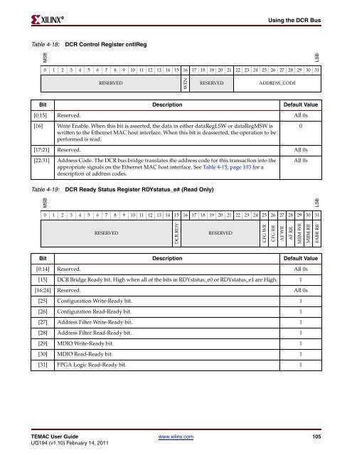
Table 4-18: DCR Control Register cntlReg<br />
MSB<br />
.<br />
Using the DCR Bus<br />
0 1 2 3 4 5 6 7 8 9 10 11 12 13 14 15 16 17 18 19 20 21 22 23 24 25 26 27 28 29 30 31<br />
RESERVED<br />
TE<strong>MAC</strong> User Guide www.xilinx.com 105<br />
<strong>UG194</strong> (v1.10) February 14, 2011<br />
WEN<br />
RESERVED ADDRESS_CODE<br />
Bit Description Default Value<br />
[0:15] Reserved. All 0s<br />
[16] Write Enable. When this bit is asserted, the data in either dataRegLSW or dataRegMSW is<br />
written to the <strong>Ethernet</strong> <strong>MAC</strong> host interface. When this bit is deasserted, the operation to be<br />
performed is read.<br />
[17:21] Reserved. All 0s<br />
[22:31] Address Code. The DCR bus bridge translates the address code for this transaction into the<br />
appropriate signals on the <strong>Ethernet</strong> <strong>MAC</strong> host interface. See Table 4-15, page 103 for a<br />
description of address codes.<br />
Table 4-19: DCR Ready Status Register RDYstatus_e# (Read Only)<br />
MSB<br />
0<br />
All 0s<br />
0 1 2 3 4 5 6 7 8 9 10 11 12 13 14 15 16 17 18 19 20 21 22 23 24 25 26 27 28 29 30 31<br />
RESERVED<br />
DCR RDY<br />
RESERVED<br />
Bit Description Default Value<br />
[0:14] Reserved. All 0s<br />
[15] DCR Bridge Ready bit. High when all of the bits in RDYstatus_e0 or RDYstatus_e1 are High. 1<br />
[16:24] Reserved. All 0s<br />
[25] Configuration Write-Ready bit. 1<br />
[26] Configuration Read-Ready bit. 1<br />
[27] Address Filter Write-Ready bit. 1<br />
[28] Address Filter Read-Ready bit. 1<br />
[29] MDIO Write-Ready bit. 1<br />
[30] MDIO Read-Ready bit. 1<br />
[31] <strong>FPGA</strong> Logic Read-Ready bit. 1<br />
CFG WR<br />
CFG RR<br />
AF WR<br />
AF RR<br />
MIIM WR<br />
MIIM RR<br />
LSB<br />
LSB<br />
FABR RR


