

Xilinx UG194 Virtex-5 FPGA Embedded Tri-Mode Ethernet MAC ...
Xilinx UG194 Virtex-5 FPGA Embedded Tri-Mode Ethernet MAC ...
Xilinx UG194 Virtex-5 FPGA Embedded Tri-Mode Ethernet MAC ...

You also want an ePaper? Increase the reach of your titles
YUMPU automatically turns print PDFs into web optimized ePapers that Google loves.
DCR Offset<br />
0x1<br />
MSB<br />
R<br />
Using the DCR Bus<br />
4. Write to the dataRegLSW register the general address [47:32] with the write mask bit<br />
and the value of the general address table register to be accessed.<br />
5. Write to cntlReg register with the address for general address word 1 (0x38C). Set the<br />
write enable bit.<br />
6. Poll the RDYstatus_e# register until the address configuration write bit is set or wait<br />
until the DCRHOSTDONEIR interrupt is asserted.<br />
To write the general address 0xFACEDEAFCAFE to the general address table register 0x1 of<br />
E<strong>MAC</strong>1:<br />
// Write the general address[31:0] to the dataRegLSW register<br />
dcr_write(E<strong>MAC</strong>1_DCRBASEADDR + 1, 0xDEAFCAFE);<br />
// Write the address of E<strong>MAC</strong>1 General Address Word 0 register to the<br />
// cntlReg_e1 register<br />
dcr_write(E<strong>MAC</strong>1_DCRBASEADDR + 2, 0x00008388);<br />
// Poll the RDYstatus_e1 register<br />
while ( !(dcr_read(E<strong>MAC</strong>1_DCRBASEADDR + 3) & 0x00010000) );<br />
// MULTI_ADDR Register 1 of AF Block<br />
// Write the general address [47:32] with the MULTI_ADDR RNW<br />
// write mask bit deasserted to the dataRegLSW register<br />
dcr_write(E<strong>MAC</strong>1_DCRBASEADDR + 1, 0x0001FACE);<br />
// Write the address of E<strong>MAC</strong>1 General Address Word 1 register to the<br />
// cntlReg_e1 register<br />
dcr_write(E<strong>MAC</strong>1_DCRBASEADDR + 2, 0x0000838C);<br />
// Poll the RDYstatus_e1 register<br />
while ( !(dcr_read(E<strong>MAC</strong>1_DCRBASEADDR + 3) & 0x00010000) );<br />
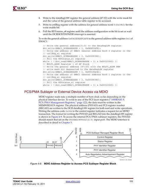
PCS/PMA Sublayer or External Device Access via MDIO<br />
MDIO register reads take a multiple number of host clock cycles depending on the<br />
physical interface device. To write to any of the PCS layer registers (“1000BASE-X<br />
PCS/PMA Management Registers,” page 122), the data must be written to the<br />
MIIMWRDATA register. The physical address (PHYAD) and PCS register number<br />
(REGAD) are written to the DCR dataRegLSW register for both read and write operations.<br />
Writing the address code 0x3B4 to the control register indicates a request for an MDIO<br />
transaction. The format for writing the PHYAD and REGAD into the dataRegLSW register<br />
is shown in Figure 4-9. To access the internal PCS/PMA sublayer registers, the PHYAD<br />
should match that set on the PHYE<strong>MAC</strong>#PHYAD[4:0] input port. The MDIO interface is<br />
described in detail in Chapter 5.<br />
0 22 26 27 31<br />
PHYAD<br />
LSB<br />
REGAD<br />
15 PCS Sublayer Managed Register Block 0<br />
Control Register<br />
PHY Identifier Register<br />
Auto-Negotiation Advertisement Register<br />
Figure 4-9: MDIO Address Register to Access PCS Sublayer Register Block<br />
<strong>UG194</strong>_4_09_072306<br />
TE<strong>MAC</strong> User Guide www.xilinx.com 111<br />
<strong>UG194</strong> (v1.10) February 14, 2011<br />
REGAD<br />
0<br />
1<br />
2<br />
3<br />
4<br />
MSB<br />
Status Register<br />
PHY Identifier Register<br />
LSB


