

Xilinx UG194 Virtex-5 FPGA Embedded Tri-Mode Ethernet MAC ...
Xilinx UG194 Virtex-5 FPGA Embedded Tri-Mode Ethernet MAC ...
Xilinx UG194 Virtex-5 FPGA Embedded Tri-Mode Ethernet MAC ...

You also want an ePaper? Increase the reach of your titles
YUMPU automatically turns print PDFs into web optimized ePapers that Google loves.
Chapter 4: Host/DCR Bus Interfaces<br />
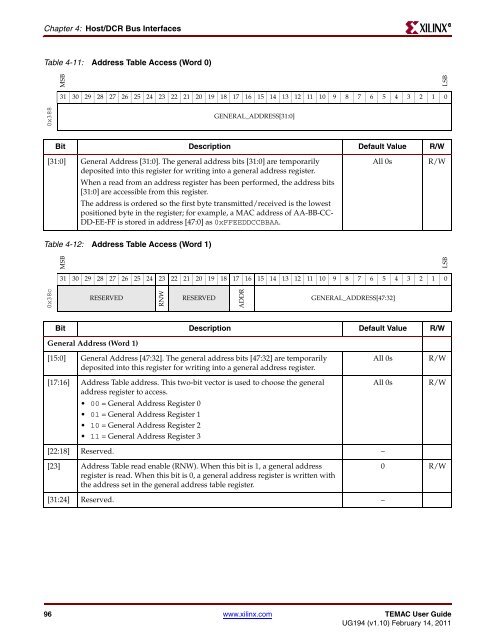
Table 4-11: Address Table Access (Word 0)<br />
0x388<br />
MSB<br />
31 30 29 28 27 26 25 24 23 22 21 20 19 18 17 16 15 14 13 12 11 10 9 8 7 6 5 4 3 2 1 0<br />
GENERAL_ADDRESS[31:0]<br />
Bit Description Default Value R/W<br />
[31:0] General Address [31:0]. The general address bits [31:0] are temporarily<br />
deposited into this register for writing into a general address register.<br />
When a read from an address register has been performed, the address bits<br />
[31:0] are accessible from this register.<br />
The address is ordered so the first byte transmitted/received is the lowest<br />
positioned byte in the register; for example, a <strong>MAC</strong> address of AA-BB-CC-<br />
DD-EE-FF is stored in address [47:0] as 0xFFEEDDCCBBAA.<br />
Table 4-12: Address Table Access (Word 1)<br />
0x38c<br />
MSB<br />
96 www.xilinx.com TE<strong>MAC</strong> User Guide<br />
<strong>UG194</strong> (v1.10) February 14, 2011<br />
LSB<br />
All 0s R/W<br />
31 30 29 28 27 26 25 24 23 22 21 20 19 18 17 16 15 14 13 12 11 10 9 8 7 6 5 4 3 2 1 0<br />
RESERVED<br />
RNW<br />
RESERVED<br />
ADDR<br />
GENERAL_ADDRESS[47:32]<br />
Bit Description Default Value R/W<br />
General Address (Word 1)<br />
[15:0] General Address [47:32]. The general address bits [47:32] are temporarily<br />
deposited into this register for writing into a general address register.<br />
[17:16] Address Table address. This two-bit vector is used to choose the general<br />
address register to access.<br />
00 = General Address Register 0<br />
01 = General Address Register 1<br />
10 = General Address Register 2<br />
11 = General Address Register 3<br />
[22:18] Reserved. –<br />
[23] Address Table read enable (RNW). When this bit is 1, a general address<br />
register is read. When this bit is 0, a general address register is written with<br />
the address set in the general address table register.<br />
[31:24] Reserved. –<br />
LSB<br />
All 0s R/W<br />
All 0s R/W<br />
0 R/W<br />
R


