- Page 1 and 2:
SÉANCE D'OUVERTURE / OPENING SESSI
- Page 3 and 4:
A l’aube de ce siècle, Airbus s
- Page 5 and 6:
Etape 4 : L’avion réel une fois
- Page 7 and 8:
C’est, sur l’exemple des essais
- Page 9 and 10:
parfois même sous la forme de plat
- Page 11 and 12:
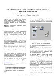
oth the system and the manufacturin
- Page 13 and 14:
Such an interdependence between tes
- Page 15 and 16:
eference books, but it is as fundam
- Page 17 and 18:
BACK MANAGEMENT DES ESSAIS SYSTEME
- Page 19 and 20:
BACK ESSAIS D’ENSEMBLE LANCEURS C
- Page 21 and 22:
Elle ne doit cependant pas être me
- Page 23 and 24:
- le plan de mesures est conséquen
- Page 25 and 26:
4.2 MAQUETTE DYNAMIQUE ARIANE 5 Dan
- Page 27 and 28:
Les points délicats liés à l’o
- Page 29 and 30:
Processus Commande Architecture Int
- Page 31 and 32:
BACK 1 Introduction AIRBUS AIRCRAFT
- Page 33 and 34:
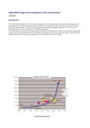
So, different test tools shall be d
- Page 35 and 36:
3.4 Architecture of A380 Simulators
- Page 37 and 38:
3.6 A380: Models In order to suppor
- Page 39 and 40:
GENERAL PRESENTATION OF JUZZLE GENE
- Page 41 and 42:
Figure 3 : Graphic User Interface o
- Page 43 and 44:
IMPLEMENTATION AND SIMULATION OF A
- Page 45 and 46:
REFERENCES [1] Space engineering, R
- Page 47 and 48:
Client Compliance Matrix (par rappo
- Page 49 and 50:
SESSION 2 : TECHNIQUES ET MOYENS D'
- Page 51 and 52:
POSTE INE A380 Les besoins fonction
- Page 53 and 54:
Les principes de l’architecture :
- Page 55 and 56:
Les éléments de l’architecture
- Page 57 and 58:
BACK Trajectographie temps réel DG
- Page 59 and 60:
Deux précisions temps réel sont p
- Page 61 and 62:
4.00 3.00 2.00 1.00 0.00 -1.00 -2.0
- Page 63 and 64:
CONCLUSION La phase d'essais en vol
- Page 65 and 66:
RÉSUMÉ: Osiris est une gamme de m
- Page 67 and 68:
1. INTRODUCTION Dassault Aviation e
- Page 69 and 70:
Exemple de modules banc d'intégrat
- Page 71 and 72:
éduction de durée des essais par
- Page 73 and 74:
5. EXEMPLE L'OSIRIS MULTIFONCTION U
- Page 75 and 76:
6. LA MODULARITÉ DE LA GAMME OSIRI
- Page 77 and 78:
• JBUILDER • ORACLE Cette modul
- Page 79 and 80:
• VX Wxorks reste l'OS de la part
- Page 81 and 82:
6.5 Exemple d'interconnexion avec d
- Page 83 and 84:
PRINCIPE 7.3 Exemple de réalisatio
- Page 85 and 86:
8. LA NOUVELLE GAMME SUR PC: VÉNUS
- Page 87 and 88:
• Un IHM de sélection des param
- Page 89 and 90:
9. CONCLUSION OSIRIS a maintenant g
- Page 91 and 92:
TABLE DES MATIERES 1. LE DATA-LINK
- Page 93 and 94:
AVIONS appartenant au réseau 25_P_
- Page 95 and 96:
• Les données à émettre sur le
- Page 97 and 98:
• 25_P_2/04 PCM émis par l'avion
- Page 99 and 100:
3.2 Le temps différé • En temps
- Page 101 and 102:
4. CONCLUSION • Toutes les IHM in
- Page 103 and 104:
INTRODUCTION Pour définir des proc
- Page 105 and 106:
- Ecarts de position en temps réel
- Page 107:
ANNEXE 1 CONSTITUTION CONSTITUTION
- Page 110 and 111:
They however incorporate some eleme
- Page 112 and 113:
As technology evolves, the boundary
- Page 114 and 115:
shown below together with the AGE c
- Page 116 and 117:
BACK ESSAIS SYSTEME SUR LES PROJETS
- Page 118 and 119:
3 qui contient le logiciel de vol.
- Page 120 and 121:
5 • essais en station « in vivo
- Page 122 and 123:
Avis, options et recommandations (5
- Page 124 and 125:
BACK Automatic Validation of Flight
- Page 126 and 127:
− The second level provides all d
- Page 128 and 129:
The operational flexibility of SINU
- Page 130 and 131:
• Test duration is reduced : for
- Page 132 and 133:
mimics from CCS ones. The objective
- Page 134 and 135:
1. Introduction ...................
- Page 136 and 137:
2. Présentation Le segment sol Ste
- Page 138 and 139:
AUS Station STA TM/TC Station STS T
- Page 140 and 141:
• La Commission de Revue d’Essa
- Page 142 and 143:
Certains essais particuliers liés
- Page 144 and 145:
Id Nom flux EXP37 Plan de vol Annex
- Page 146 and 147:
TTC’2003 Stentor 10/06/2003 QUALI
- Page 148 and 149:
TTC’2003 Le Programme Stentor 10/
- Page 150 and 151:
TTC’2003 Satellite GEO TM/TC/Rang
- Page 152 and 153:
TTC’2003 •Equipes CNES : Qualif
- Page 154 and 155:
TTC’2003 •L’organisation mise
- Page 156 and 157:
TTC’2003 Interfaces Externes :
- Page 158 and 159:
TTC’2003 Les Contraintes de Déve
- Page 160 and 161:
TTC’2003 Contient ontient la la m
- Page 162 and 163:
TTC’2003 10/06/2003 Qualification
- Page 164 and 165:
TTC’2003 10/06/2003 Qualification
- Page 166 and 167:
BACK Résumé : Outil de traitement
- Page 168 and 169:
1 Principes généraux de l’outil
- Page 170 and 171:
1.2.3 Valise de piste L’outil peu
- Page 172 and 173:
2 Capacités fonctionnelles 2.1 Arc
- Page 174 and 175:
Vue f(t) 2.3.1 Vues y=f(t) Ces vues
- Page 176 and 177:
Maquette aéronef Alarmes Bar-graph
- Page 178 and 179:
2.3.3 Représentation trajectograph
- Page 180 and 181:
2.3.5 Vidéo Par ailleurs, si le ma
- Page 182 and 183:
3 Concept de structure d’accueil
- Page 184 and 185:
4 Exemples d’utilisation 4.1.1 HB
- Page 186 and 187:
SESSION 3 : Capteurs et dispositifs
- Page 188 and 189:
BACK THE NEXT GENERATION AIRBORNE D
- Page 190 and 191:
3. DC SPECIFICATIONS - SEEING THE W
- Page 192 and 193:
For the purposes of this paper it i
- Page 194 and 195:
hardware down and led to widely acc
- Page 196 and 197:
mechanism. In a system where a late
- Page 198 and 199:
0 X Y X' Y' 0 X Y Sampling Cycle X
- Page 200 and 201:
- Perform the exchange in a rigorou
- Page 202 and 203:
GLOSSARY AFDX Avionics Full DupleX
- Page 204 and 205:
The complete message is recorded by
- Page 206 and 207:
The L3 switches allow forwarding da
- Page 208 and 209:
Furthermore, the configuration of t
- Page 210 and 211:
BACK LOGICIEL JAVA D’ACQUISITION
- Page 212 and 213:
ISA ISA Interface utilisateur Objet
- Page 214 and 215:
CONCLUSION La première version de
- Page 216 and 217:
; ( ( + & 2+5. . & & , & . + & +2(
- Page 218 and 219:
( +, & + < 0 9& - & = (( + 1 - + +,
- Page 220 and 221:
BACK Telemetry Recording Workstatio
- Page 222 and 223:
Figure 1: Real-time pen tip display
- Page 224 and 225:
establishing different socket conne
- Page 226 and 227:
73 64 63 61 60 48 45 40 35 Level (d
- Page 228 and 229:
SESSION 5 : TELEMESURE (SPECTRE - M
- Page 230 and 231:
Currently various avenues are explo
- Page 232 and 233:
Binary X Binary to RNS and RNS to B
- Page 234 and 235:
The index multiplier block will be
- Page 236 and 237:
The current implementation consists
- Page 238 and 239:
Spécificité de la télémesure AI
- Page 240 and 241:
Technique COFDM : La modulation COF
- Page 242 and 243:
La réception s’effectue par une
- Page 244 and 245:
BACK ETCC'2003 European Test and Te
- Page 246 and 247:
ETCC'2003 European Test and Telemet
- Page 248 and 249:
ETCC'2003 European Test and Telemet
- Page 250 and 251:
ETCC'2003 European Test and Telemet
- Page 252 and 253:
SESSION 6 : SYSTEMES DE TELEMESURE
- Page 254 and 255:
f f p IF = R b = 4R b ∆f = 0. 7R
- Page 256 and 257:
2.3 ADC Fig.5 (a) y (t) and its spe
- Page 258 and 259:
2.5 FM demodulation Fig.9 I ‘(nT1
- Page 260 and 261:
References 1. Gardner FM. A BPSK/QP
- Page 262 and 263:
L/S/C /X/Ku /Ka band Spacelink Syst
- Page 264 and 265:
Spacelink System - The solution for
- Page 266 and 267:
SPOT Σ ∆ X band feed Data LNA Tr
- Page 268 and 269:
défilant. Le cahier des charges d
- Page 270 and 271:
TOURELLE HEXAPODE La tourelle hexap
- Page 272 and 273:
Ci après, tableau des spécificati
- Page 274 and 275:
BACK CRISTAUX PHOTONIQUES ET METAMA
- Page 276 and 277:
BACK Systems, Design & Tests Direct
- Page 278 and 279:
1. INTRODUCTION Cette communication
- Page 280 and 281:
Figure 2-1 Vue générale de la Bas
- Page 282 and 283:
3. ETALONNAGE DE LA BASE 3.1 PRINCI
- Page 284 and 285:
Par définition, le taux de polaris
- Page 286 and 287:
This document is the property of EA
- Page 288 and 289:
amplitude (dB) 10 0 -10 -20 -30 -40
- Page 290 and 291:
amplitude (dB) 10 0 -10 -20 -30 -40
- Page 292 and 293:
V1=K1.GVV.E.{[cos()-.sin()] + 1_vra
- Page 294 and 295:
Quelques calculs d’incertitude so
- Page 296 and 297:
- 21 - Amplitude polarisation verti
- Page 298 and 299:
- 23 - Amplitude composante vertica
- Page 300 and 301:
- 25 - Amplitude composante vertica
- Page 302 and 303:
3.4 SYNTHESE DES RESULTATS CONCERNA
- Page 304 and 305:
4.2 DEFINITION DE L'ANTENNE DE MISE
- Page 306 and 307:
4.4 DEFINITION DE L'ANTENNE DE REFE
- Page 308 and 309:
5.1.2 Diagrammes de rayonnement 5.1
- Page 310 and 311:
5.2 ANTENNE DE REFERENCE BANDE P 5.
- Page 312 and 313:
Gain (dBi) 5.2.2.2 Résultats Ils s
- Page 314 and 315:
Comme attendu, la coupe xOz présen
- Page 316 and 317:
Gain (dBi) 5.3.2 diagramme de rayon
- Page 318 and 319:
Gain (dBi) 15 10 5 0 -5 -10 -15 -20
- Page 320 and 321:
BACK INTRODUCTION MESURE DE CHAMP P
- Page 322 and 323:
MESURE DE CHAMP PAR SYSTEME PORTABL
- Page 324 and 325:
MESURE DE CHAMP PAR SYSTEME PORTABL
- Page 326 and 327:
Abstract Helicopters are relatively
- Page 328 and 329:
Au sol, la station réceptionne le
- Page 330 and 331:
BACK Résumé Architecture d’une
- Page 332 and 333:
Architecture type lanceur lourd ARI
- Page 334 and 335:
Architecture petit lanceur L’arch
- Page 336 and 337:
Diagramme de l’UCTM Voies analogi
- Page 338 and 339:
Exemples de capteurs utilisés Type
- Page 340 and 341:
SESSION 8 : COMPATIBILITE ELECTROMA
- Page 342 and 343:
1. CONTEXTE GENERAL Le durcissement
- Page 344 and 345:
Figure 1 : Actions de qualification
- Page 346 and 347:
5. LES PARAMETRES D’OPTIMISATION
- Page 348 and 349:
7. PERFORMANCE ET OPTIMISATION DU P
- Page 350 and 351:
La qualification du durcissement re
- Page 352 and 353:
UNIT Unit EMC documents : - groundi
- Page 354 and 355:
At equipment level EMC TEST PROGRAM
- Page 356 and 357:
BACK ETTC 2003. Le rôle de la simu
- Page 358 and 359:
comprenant des objets complexes, n
- Page 360 and 361:
Cette approche permet, avec les mê
- Page 362 and 363:
Les Thèses ONERA UPS Prise en comp
- Page 364 and 365:
Pression Ligne bifilaire non blind
- Page 366 and 367:
1.8 1,8 Tension continue V 1.6 1.4
- Page 368 and 369:
270 Ω I0 IL 2,7 kΩ (b) Alimenta
- Page 370 and 371:
What is the budget of the statistic
- Page 372 and 373:
Monte Carlo approach: This is a thr
- Page 374 and 375:
2 Etat de l’art des standards de
- Page 376 and 377:
2.1.6 Emissions standards 61967 par
- Page 378 and 379:
- Limites pour l’immunité DPI (e
- Page 380 and 381:
PRESENTATIONS POSTER / POSTER PRESE
- Page 382 and 383:
BACK LA TELEMESURE SUR AIRBUS JC GH
- Page 384 and 385:
Dans le cycle d ’essais en vol ,
- Page 386 and 387:
CONCLUSION - NOS BESOINS FUTURS AIR
- Page 388 and 389:
LOGICIELS DE MESURE ET DE TRAITEMEN
- Page 390 and 391:
LOGICIELS DE MESURE ET DE TRAITEMEN
- Page 392 and 393:
LOGICIELS DE MESURE ET DE TRAITEMEN
- Page 394 and 395:
In order to optimize the phase nois
- Page 396 and 397:
Photo-oscillator active device Opti
- Page 398 and 399:
the inverse of N×N correlation mat
- Page 400 and 401:
quasi-synchronous multiuser detecto
- Page 402 and 403:
Multiuser Interference Canceler ”
- Page 404 and 405:
the inverse of N×N correlation mat
- Page 406 and 407:
quasi-synchronous multiuser detecto
- Page 408 and 409: Multiuser Interference Canceler ”
- Page 410 and 411: All these sub-systems can be easily
- Page 412 and 413: 3.5 ACPR RACK Gateway and satellite
- Page 414 and 415: 4.2 COMPONENT DEGRADATION MEASUREME
- Page 416 and 417: Indeed, when the objective of the t
- Page 418 and 419: All the five points can be achieved
- Page 420 and 421: M r Mmax (0 dB, -180°) b = 0 a ωc
- Page 422 and 423: 2 - Test devices at ENSICA Souffler
- Page 424 and 425: Soufflerie à Densité Variable (SD
- Page 426 and 427: Capacité : - pour la charge axiale
- Page 428 and 429: Machine d’essai de fatigue en fle
- Page 430 and 431: torsion. - asservissement de chaque
- Page 432 and 433: KEY 1 WORD IENA PACKET format An IE
- Page 434 and 435: TD: “0” means that the paramete
- Page 436 and 437: PARAMETER DESCRIPTION This array de
- Page 438 and 439: BACK UTILISATION de CAMERAS NUMERIQ
- Page 440 and 441: TABLE DES MATIÈRES 1. INTRODUCTION
- Page 442 and 443: 2. CONTEXTE DES ESSAIS Le but des e
- Page 444 and 445: 3. LES BESOINS ET LES CONTRAINTES 3
- Page 446 and 447: 4. CHOIX DE LA CAMERA 4.1 Démarche
- Page 448 and 449: 5.1.4 Adaptations Les deux principa
- Page 450 and 451: Tir d'un missile AIR/AIR éjecté T
- Page 452 and 453: 6. CONCLUSION Cette évaluation mon
- Page 454 and 455: Capteur Intelligent IEEE 1451.4 Pri
- Page 456 and 457: pC/g Piezo Accelerometer mV/g Piezo
- Page 460 and 461: 4.2. Sensitivity according to the h
- Page 462 and 463: BACK STUDY OF 3∆t PASSIVE LOCATIN
- Page 464 and 465: ∆t 1 ∆t ∆t 2 = t = t M N −1
- Page 466 and 467: For the speed of the reentry vehicl
- Page 468 and 469: BACK TITLE In orbit satellite Gain
- Page 470 and 471: dBm dBm Results obtain with the con
- Page 472 and 473: 3. NEW METHOD DEVELOPPED FOR IOT SA
- Page 474 and 475: The following figures present the g
- Page 476 and 477: 3.2 Analysis of the contribution Th
- Page 478 and 479: ETSC Annual Activities Gerhard Maye
- Page 480 and 481: BACK Abstract European Telemetry St
- Page 482 and 483: The file structure is also adopted
- Page 484 and 485: BACK The statistical Evaluation Of
- Page 486 and 487: BACK Abstract Vendor Independent Da