- Page 2 and 3:
COLLECTION OF PAPERS PRESENTED AT T
- Page 4 and 5:
III
- Page 6 and 7:
V
- Page 8 and 9:
Table of Contents Wednesday 11 May
- Page 10 and 11:
PANEL DISCUSSION TEXTILE MICROSYSTE
- Page 12 and 13:
Friday 13 May SESSION C4: APPLICATI
- Page 14 and 15:
SPECIAL SESSION OF BIO-MEMS/NEMS a
- Page 16 and 17:
11-13 May 2011, Aix-en-Provence, Fr
- Page 18 and 19:
11-13 May 2011, Aix-en-Provence, F
- Page 20 and 21:
11-13 May 2011, Aix-en-Provence, F
- Page 22 and 23:
11-13 May 2011, Aix-en-Provence, F
- Page 24 and 25:
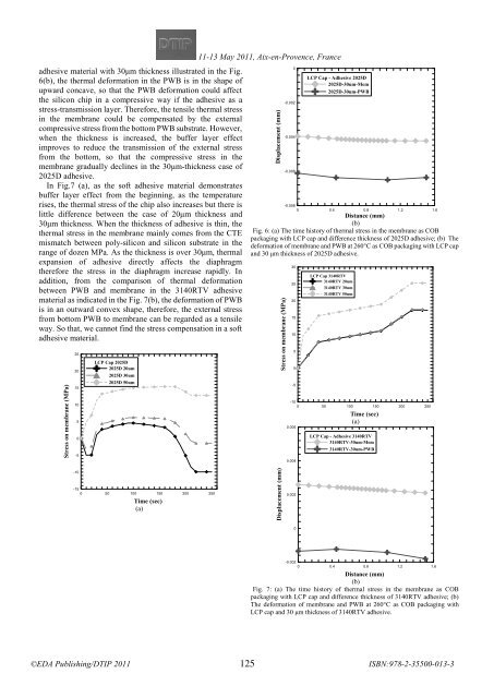
suspended membrane can be pulled to
- Page 26 and 27:
most likely due to not yet consider
- Page 28 and 29:
11-13 May 2011, Aix-en-Provence, F
- Page 30 and 31:
that detectors may measure the diff
- Page 32 and 33:
2) Cavity width effect To verify th
- Page 34 and 35:
11-13 May 2011, Aix-en-Provence, Fr
- Page 36 and 37:
Fig.9. Capacitive sensor output, Va
- Page 38 and 39:
11-13 May, 2011, Aix-en-Provence,
- Page 40 and 41:
The anode and cathode are connected
- Page 42 and 43:
11-13 May , 2011 , Aix-en-Provence,
- Page 44 and 45:
11-13 May 2011, Aix-en-Provence, F
- Page 46 and 47:
11-13 May 2011, Aix-en-Provence, Fr
- Page 48 and 49:
11-13 May 2011, Aix-en-Provence, F
- Page 50 and 51:
! 11-13 May 2011, Aix-en-Provence,
- Page 52 and 53:
! 11-13 May 2011, Aix-en-Provence,
- Page 54 and 55:
! TABLE 3 SUMMARY OF SELECTIVITIES
- Page 56 and 57:
11-13 May 2011, Aix-en-Provence, Fr
- Page 58 and 59:
11-13 May 2011, Aix-en-Provence, Fr
- Page 60 and 61:
11-13 May 2011, Aix-en-Provence, Fr
- Page 62 and 63:
The fabrication of optical Cap-Wafe
- Page 64 and 65:
the glass is polished down in a cos
- Page 66 and 67:
11-13 May 2011, Aix-en-Provence, Fr
- Page 68 and 69:
11-13 May 2011, Aix-en-Provence, F
- Page 70 and 71:
11-13 May 2011, Aix-en-Provence, F
- Page 72 and 73:
Fig. 14. Time history of the envelo
- Page 74 and 75:
11-13 May 2011, Aix-en-Provence, F
- Page 76 and 77:
11-13 May 2011, Aix-en-Provence, Fr
- Page 78 and 79:
We have reported that how base mode
- Page 80 and 81:
We assume that 11-13 May 2011, Aix
- Page 82 and 83:
11-13 May 2011, Aix-en-Provence, F
- Page 84 and 85:
Y X Fig. 1. Scanning electron mic
- Page 86 and 87:
10 3 11-13 May 2011, Aix-en-Proven
- Page 88 and 89:
Intenstiy (counts/second) Fig. 1. X
- Page 90 and 91: 11-13 May 2011, Aix-en-Provence, Fr
- Page 92 and 93: 11-13 May 2011, Aix-en-Provence, Fr
- Page 94 and 95: etween x 2 to L (remember that x 2
- Page 96 and 97: 11-13 May 2011, Aix-en-Provence, F
- Page 98 and 99: 11-13 May 2011, Aix-en-Provence, F
- Page 100 and 101: 11-13 May 2011, Aix-en-Provence, Fr
- Page 102 and 103: 11-13 May 2011, Aix-en-Provence, Fr
- Page 104 and 105: 11-13 May 2011, Aix-en-Provence, F
- Page 106 and 107: piezoelectric displacement transduc
- Page 108 and 109: Figure 7 Displacement conditions of
- Page 110 and 111: protect the corners from undercut.
- Page 112 and 113: 11-13 May 2011, Aix-en-Provence, F
- Page 114 and 115: A. Continuous domain Starting from
- Page 116 and 117: Fig. 8. Central finite difference m
- Page 118 and 119: 11-13 May 2011, Aix-en-Provence, F
- Page 120 and 121: 700 11-13 May 2011, Aix-en-Provenc
- Page 122 and 123: o o o o o o o o Check applicability
- Page 124 and 125: C. Identification Results The ident
- Page 126 and 127: The proposed solution for this prob
- Page 128 and 129: teen wire segments of a coil, as in
- Page 130 and 131: As the metallization is too reflect
- Page 132 and 133: B. Implemented die overview A die c
- Page 134 and 135: 11-13 May 2011, Aix-en-Provence, F
- Page 136 and 137: IN CLK OUT Fig. 16. Probe setup for
- Page 138 and 139: 11-13 May 2011, Aix-en-Provence, F
- Page 142 and 143: 11-13 May 2011, Aix-en-Provence, F
- Page 144 and 145: 11-13 May 2011, Aix-en-Provence, F
- Page 146 and 147: B. Dynamics of Energy Flows For a l
- Page 148 and 149: 11-13 May 2011, Aix-en-Provence, F
- Page 150 and 151: 11-13 May 2011, Aix-en-Provence, F
- Page 152 and 153: 11-13 May, Aix-en-Provence, France
- Page 154 and 155: 80˚C. Additionally, we looked into
- Page 156 and 157: The XRD shows a peak above the 2θ
- Page 158 and 159: fibers which define the electric co
- Page 160 and 161: 11-13 May 2011, Aix-en-Provence, Fr
- Page 162 and 163: Figure 15. Key board input system.
- Page 164 and 165: ρ = h 2∆α∆T + + E 1h 3 1 +E 2
- Page 166 and 167: 11-13 May 2011, Aix-en-Provence, Fr
- Page 168 and 169: In recent years, the pipe flow moni
- Page 170 and 171: As the speed of the rotor increases
- Page 172 and 173: 11-13 May 2011, Aix-en-Provence, F
- Page 174 and 175: 11-13 May 2011, Aix-en-Provence, Fr
- Page 176 and 177: inches silicon wafers which have th
- Page 178 and 179: samples tested in different vacuum
- Page 180 and 181: l c 11-13 May 2011, Aix-en-Provence
- Page 182 and 183: Vp (V) 3,5 3,0 2,5 2,0 1,5 1,0 0,5
- Page 184 and 185: 11-13 May 2011, Aix-en-Provence, Fr
- Page 186 and 187: II. MATHEMATICAL MODEL AND NUMERICA
- Page 188 and 189: fluids travel along a curved channe
- Page 190 and 191:
measured mixing indices are depicte
- Page 192 and 193:
length, which enables them to focus
- Page 194 and 195:
11-13 May 2011, Aix-en-Provence, F
- Page 196 and 197:
however, a rotation for coincidence
- Page 198 and 199:
11-13 May 2011, Aix-en-Provence, F
- Page 200 and 201:
11-13 May 2011, Aix-en-Provence, F
- Page 202 and 203:
11-13 May 2011, Aix-en-Provence, F
- Page 204 and 205:
excludes the nature of the fixed bo
- Page 206 and 207:
Using the radial and tangential mid
- Page 208 and 209:
11-13 May 2011, Aix-en-Provence, F
- Page 210 and 211:
11-13 May 2011, Aix-en-Provence, F
- Page 212 and 213:
11-13 May 2011, Aix-en-Provence, F
- Page 214 and 215:
11-13 May 2011, Aix-en-Provence, F
- Page 216 and 217:
Now the challenge in data handling
- Page 218 and 219:
value of every active channel. Ther
- Page 220 and 221:
11-13 May 2011, Aix-en-Provence, F
- Page 222 and 223:
11-13 May, Aix-en-Provence, France
- Page 224 and 225:
11-13 May, Aix-en-Provence, France
- Page 226 and 227:
11-13 May 2011, Aix-en-Provence, Fr
- Page 228 and 229:
11-13 May 2011, Aix-en-Provence, Fr
- Page 230 and 231:
electrocardiogram. • The heart be
- Page 232 and 233:
11-13 May 2011, Aix-en-Provence, F
- Page 234 and 235:
In our work, we proposed an innovat
- Page 236 and 237:
Fig. 8 Concept of the in-home perso
- Page 238 and 239:
found that the early-stage diagnosi
- Page 240 and 241:
11-13 May 2011, Aix-en-Provence, F
- Page 242 and 243:
11-13 May 2011, Aix-en-Provence, F
- Page 244 and 245:
Power monitoring data detected by w
- Page 246 and 247:
11-13 May 2011, Aix-en-Provence, F
- Page 248 and 249:
device consisted of a bimorph canti
- Page 250 and 251:
where C others is the capacitance o
- Page 252 and 253:
11-13 May 2011, Aix-en-Provence, F
- Page 254 and 255:
11-13 May 2011, Aix-en-Provence, F
- Page 256 and 257:
11-13 May 2011, Aix-en-Provence, F
- Page 258 and 259:
operation, the pressure inside the
- Page 260 and 261:
11-13 May 2011, Aix-en-Provence, F
- Page 262 and 263:
increased. 11-13 May 2011, Aix-en-
- Page 264 and 265:
11-13 May 2011, Aix-en-Provence, F
- Page 266 and 267:
coefficient compatible with the mic
- Page 268 and 269:
11-13 May 2011, Aix-en-Provence, F
- Page 270 and 271:
Variable Description Value Crab-leg
- Page 272 and 273:
11-13 May 2011, Aix-en-Provence, F
- Page 274 and 275:
11-13 May 2011, Aix-en-Provence, F
- Page 276 and 277:
Membrane weight (mg) Fig. 4. Struct
- Page 278 and 279:
11-13 May 2011, Aix-en-Provence, F
- Page 280 and 281:
11-13 May 2011, Aix-en-Provence, F
- Page 282 and 283:
So far, the expected major contribu
- Page 284 and 285:
al. used a modified LIGA (German ac
- Page 286 and 287:
11-13 May 2011, Aix-en-Provence, F
- Page 288 and 289:
11-13 May 2011, Aix-en-Provence, F
- Page 290 and 291:
11-13 May 2011, Aix-en-Provence, F
- Page 292 and 293:
REFERENCES [1] G. Mehta, J. Lee, W.
- Page 294 and 295:
11-13 May 2011, Aix-en-Provence, F
- Page 296 and 297:
followed by titanium (Ti) which sho
- Page 298 and 299:
exposure dose, post exposure bake t
- Page 300 and 301:
#### ##/&### 3 # #
- Page 302 and 303:
*5%6,+/.,-,7-, ,+.,1/21* %
- Page 304 and 305:
B. Energy Applications Society is f
- Page 306 and 307:
11-13 May 2011, Aix-en-Provence, Fr
- Page 308 and 309:
11-13 May 2011, Aix-en-Provence, Fr
- Page 310 and 311:
11-13 May 2011, Aix-en-Provence, F
- Page 312 and 313:
11-13 May 2011, Aix-en-Provence, F
- Page 314 and 315:
Presently, the microfabrication pro
- Page 316 and 317:
[6] C. Richard, A. Renaudin, V. Aim
- Page 318 and 319:
NA sinθ c 11-13 May 2011, Aix-en-
- Page 320 and 321:
the waveguide on the fused silica,
- Page 322 and 323:
microphone diaphragm. The chosen CM
- Page 324 and 325:
11-13 May 2011, Aix-en-Provence, F
- Page 326 and 327:
TABLE V MICROPHONE CHARACTERISTICS
- Page 328 and 329:
11-13 May 2011, Aix-en-Provence, F
- Page 330 and 331:
Figure 7b shows the effect of a par
- Page 332 and 333:
11-13 May 2011, Aix-en-Provence, F
- Page 334 and 335:
over the temperature range (i.e. th
- Page 336 and 337:
11-13 May 2011, Aix-en-Provence, F
- Page 338 and 339:
11-13 May 2011, Aix-en-Provence, F
- Page 340 and 341:
given. This allows a CTM model to b
- Page 342 and 343:
11-13 May 2011, Aix-en-Provence, F
- Page 344 and 345:
11-13 May 2011, Aix-en-Provence, F
- Page 346 and 347:
11-13 May 2011, Aix-en-Provence, F
- Page 348 and 349:
the magic-Tee, and the coherent sig
- Page 350 and 351:
11-13 May 2011, Aix-en-Provence, F
- Page 352 and 353:
After analyzing the two conditions
- Page 354 and 355:
IV. MICRO FABRICATION For fabricati
- Page 356 and 357:
11-13 May 2011, Aix-en-Provence, F
- Page 358 and 359:
IV. A. Simulation and Sensitivity A
- Page 360 and 361:
11-13 May 2011, Aix-en-Provence, Fr
- Page 362 and 363:
11-13 May 2011, Aix-en-Provence, Fr
- Page 364 and 365:
11-13 May 2011, Aix-en-Provence, Fr
- Page 366 and 367:
grown to sub-confluence were washed
- Page 368 and 369:
11-13 May 2011, Aix-en-Provence, F
- Page 370 and 371:
Clamps rotation [21] Clamps transla
- Page 372 and 373:
Layout Total dimensions of the grip
- Page 374 and 375:
11-13 May 2011, Aix-en-Provence, F
- Page 376 and 377:
focusing increased both as the stre
- Page 378 and 379:
11-13 May, 2011, Aix-en-Provence,
- Page 380 and 381:
Time of diffusion (hr) 1200 1000 80
- Page 382 and 383:
11-13 May, 2011, Aix-en-Provence,
- Page 384 and 385:
11-13 May 2011, Aix-en-Provence, F
- Page 386 and 387:
Chip Magnet Light source Hot plate
- Page 388 and 389:
above, they would move to upward an
- Page 390 and 391:
11-13 May 2011, Aix-en-Provence, F
- Page 392 and 393:
11-13 May 2011, Aix-en-Provence, F
- Page 394 and 395:
11-13 May, 2011, Aix-en-Provence,
- Page 396 and 397:
11-13 May, 2011, Aix-en-Provence,
- Page 398 and 399:
11-13 May, 2011, Aix-en-Provence,
- Page 400 and 401:
This phenomenon is now reaching the
- Page 402 and 403:
C. Proof mass displacement Moreover
- Page 404 and 405:
11-13 May 2011, Aix-en-Provence, Fr
- Page 406 and 407:
11-13 May 2011, Aix-en-Provence, Fr
- Page 408 and 409:
The VerilogA block code is : 11-13
- Page 410 and 411:
Author Index Abi-Saab D. 81 Aimez V
- Page 412:
Nussbaum Dominic 273 O’Hara T. 35