

Online proceedings - EDA Publishing Association
Online proceedings - EDA Publishing Association
Online proceedings - EDA Publishing Association

You also want an ePaper? Increase the reach of your titles
YUMPU automatically turns print PDFs into web optimized ePapers that Google loves.
and far away from the pillar (7.47µm at 40µm from the left<br />
side pillar).<br />
The flow of the resist along the pillar during lamination is<br />
the major difficulty we have encountered during the<br />
development of this process. In order to avoid this problem,<br />
we have optimized process parameters. Figure 8 shows an<br />
example of flowing effect. This problem becomes really<br />
significant when microstructures have low dimensions as it<br />
reduces drastically the volume of encapsulated fluid. In our<br />
case it has been considered negligible regarding the final<br />
volume of each structure (1800µl). However, this<br />
phenomenon has been reduced by increasing the soft bake<br />
time (near twice the initial value) and by lowering the<br />
pressure and speed lamination to the minimum value<br />
allowed by the laminator. It has been tried to increase the<br />
thickness of the plastic layer which supports the resist but<br />
no improvement has been observed.<br />
11-13 <br />
May 2011, Aix-en-Provence, France<br />
<br />
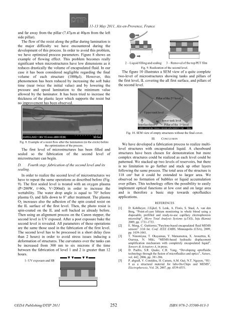
2 – Liquid filling and sealing 3 – Removal of the top PET film<br />
Fig. 9. Realization of the second level.<br />
The figure 10 illustrates a SEM view of a quite complete<br />
two-level of microstructures showing tanks and pillars of<br />
the first level, IL covering the all first surface, and pillars of<br />
the second level.<br />
Pillar of the 2 nd level<br />
Upper tank level<br />
Interface layer<br />
lower tank level<br />
Pillar of the 1 st level<br />
Fig. 10. SEM view of empty structures without the final cover.<br />
Fig. 8. Example of a resist flow after the lamination (in the circle) before<br />
the optimization of the process.<br />
The first level of microstructures has been filled and<br />
sealed so the fabrication of the second level of<br />
microstructure can begin.<br />
D. Fourth step: fabrication of the second level and its<br />
sealing.<br />
In order to realize the second level of microstructures we<br />
have to repeat the same operations as described before (Fig.<br />
9). The first sealed level is treated with an oxygen plasma<br />
(P=200W, t=60s, V=200ml) in order to increase the<br />
wettability. The water drop angle is equal to 70° before<br />
plasma O 2 and falls down to 8° after treatment. The plasma<br />
O 2 increases also the adhesion of the spin coated resist on<br />
the IL surface of the first level. Then, the photo resist is<br />
spin-coated on the IL and soft backed as already before.<br />
Then using an alignment process on the Canon stepper, the<br />
second level is UV exposed. After a post exposure bake the<br />
second level is revealed. All parameters of these operations<br />
are the same those used in the fabrication of the first level.<br />
The second level has to be processed in a short delay (less<br />
than 2 hours) in order to avoid stress issues inducing a<br />
deformation of structures. The curvatures over the tanks can<br />
be increased from 300 nm to six microns if the time<br />
between the fabrication of level 1 and 2 is greater than 12<br />
hours.<br />
1- UV exposure and SB<br />
III. CONCLUSION<br />
We have developed a fabrication process to realize multilevel<br />
structures with encapsulated liquid. A chessboard<br />
structures have been chosen for demonstration but more<br />
complex structures could be realized as each level could be<br />
patterned. We stacked up two levels of reservoirs, but there<br />
is no limitation to go further and stack up other layers<br />
following the same process. The total area of the structure is<br />
118 cm² but it could be extended to larger area. We<br />
observed no formation of bubbles or liquid accumulation<br />
over pillars. This technology offers the possibility to easily<br />
implement optical functions at low cost and on large area<br />
and is therefore a basic step towards optofluidics<br />
applications.<br />
REFERENCES<br />
[1] D. Kohlheyer, J.Eijkel, S. Lenk, A. Floris, S. Staal, A. van den<br />
Berg, “Point-of-care lithium monitoring in whole blood using a<br />
disposable, prefilled and ready-to-use capillary electrophoresis<br />
microchip”, Micro Total Analysis Systems (µTAS), Jeju (Korea)<br />
2009, pp. 1731-1733.<br />
[2] E. Meng, C. Guttierrez,”Parylene-based encapsulated fluid MEMS<br />
sensors” 31th Int. Conf. IEEE EMBS, Minneapolis (USA), 2009,<br />
pp. 1039-1041.<br />
[3] T. Ninomiyaa, T. Okayamaa, Y. Matsumotoa, X. Arouettea, K.<br />
Osawaa, N. Miki, “MEMS-based hydraulic displacement<br />
amplification mechanism with completely encapsulated liquid”.<br />
Sensors & Actuators A, in press.<br />
[4] D. Psaltis, S.R. Quake, C.H. Yang, “Developeng optofluidic<br />
technology through the fusion of microfluidics and optics”, Nature,<br />
vol. 442, 2006, pp. 381-386.<br />
[5] P. abgrall, V. Conédéra, H. Camon, A.M. Gué, N.T. Nguyen, “SU-<br />
8 as a structural material for labs-On-Chips and MEMS”,<br />
Electrophoresis, Vol. 28, 2007, pp. 4539-4551.<br />
252


