

Online proceedings - EDA Publishing Association
Online proceedings - EDA Publishing Association
Online proceedings - EDA Publishing Association

Create successful ePaper yourself
Turn your PDF publications into a flip-book with our unique Google optimized e-Paper software.
eam to improve the electrical contacts and to solve the<br />
problems of oxidation caused by humidity which disturb and<br />
stick beams (the metal wall covering is explained in [4,5]).<br />
Thanks to platinum the reliability and the yield of NS devices<br />
was clearly improved [5].<br />
11-13 May 2011, Aix-en-Provence, France<br />
<br />
<br />
ACKNOWLEDGEMENT<br />
Samples were fabricated and designed by Stanford<br />
University. They were finalized and customized at the<br />
Grenoble Up-line Technological Platform (PTA) which is cooperated<br />
by CEA & CNRS within the framework of the<br />
French Basic Technology Research (BTR) network. This work<br />
has been partly supported by the EU through the Network of<br />
Excellence NANOFUNCTION FP7/ICT/NoE (95145). The<br />
author would like to thank Xavier Mescot, Martin Gri, Remy<br />
Lefevre and Xin Xu for their valuable help.<br />
REFERENCES<br />
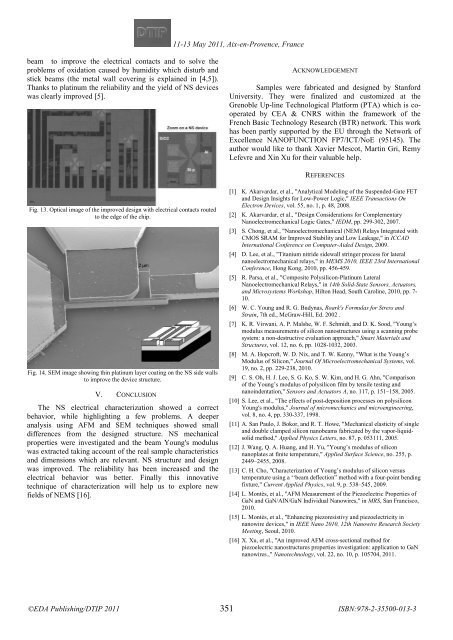
Fig. 13. Optical image of the improved design with electrical contacts routed<br />
to the edge of the chip.<br />
Fig. 14. SEM image showing thin platinum layer coating on the NS side walls<br />
to improve the device structure.<br />
V. CONCLUSION<br />
The NS electrical characterization showed a correct<br />
behavior, while highlighting a few problems. A deeper<br />
analysis using AFM and SEM techniques showed small<br />
differences from the designed structure. NS mechanical<br />
properties were investigated and the beam Young's modulus<br />
was extracted taking account of the real sample characteristics<br />
and dimensions which are relevant. NS structure and design<br />
was improved. The reliability has been increased and the<br />
electrical behavior was better. Finally this innovative<br />
technique of characterization will help us to explore new<br />
fields of NEMS [16].<br />
[1] K. Akarvardar, et al., "Analytical Modeling of the Suspended-Gate FET<br />
and Design Insights for Low-Power Logic," IEEE Transactions On<br />
Electron Devices, vol. 55, no. 1, p. 48, 2008.<br />
[2] K. Akarvardar, et al., "Design Considerations for Complementary<br />
Nanoelectromechanical Logic Gates," IEDM, pp. 299-302, 2007.<br />
[3] S. Chong, et al., "Nanoelectromechanical (NEM) Relays Integrated with<br />
CMOS SRAM for Improved Stability and Low Leakage," in ICCAD<br />
International Conference on Computer-Aided Design, 2009.<br />
[4] D. Lee, et al., "Titanium nitride sidewall stringer process for lateral<br />
nanoelectromechanical relays," in MEMS 2010, IEEE 23rd International<br />
Conference, Hong Kong, 2010, pp. 456-459.<br />
[5] R. Parsa, et al., "Composite Polysilicon-Platinum Lateral<br />
Nanoelectromechanical Relays," in 14th Solid-State Sensors, Actuators,<br />
and Microsystems Workshop, Hilton Head, South Caroline, 2010, pp. 7-<br />
10.<br />
[6] W. C. Young and R. G. Budynas, Roark's Formulas for Stress and<br />
Strain, 7th ed., McGraw-Hill, Ed. 2002 .<br />
[7] K. R. Virwani, A. P. Malshe, W. F. Schmidt, and D. K. Sood, "Young’s<br />
modulus measurements of silicon nanostructures using a scanning probe<br />
system: a non-destructive evaluation approach," Smart Materials and<br />
Structures, vol. 12, no. 6, pp. 1028-1032, 2003.<br />
[8] M. A. Hopcroft, W. D. Nix, and T. W. Kenny, "What is the Young’s<br />
Modulus of Silicon," Journal Of Microelectromechanical Systems, vol.<br />
19, no. 2, pp. 229-238, 2010.<br />
[9] C. S. Oh, H. J. Lee, S. G. Ko, S. W. Kim, and H. G. Ahn, "Comparison<br />
of the Young’s modulus of polysilicon film by tensile testing and<br />
nanoindentation," Sensors and Actuators A, no. 117, p. 151–158, 2005.<br />
[10] S. Lee, et al., "The effects of post-deposition processes on polysilicon<br />
Young's modulus," Journal of micromechanics and microengineering,<br />
vol. 8, no. 4, pp. 330-337, 1998.<br />
[11] A. San Paulo, J. Bokor, and R. T. Howe, "Mechanical elasticity of single<br />
and double clamped silicon nanobeams fabricated by the vapor-liquidsolid<br />
method," Applied Physics Letters, no. 87, p. 053111, 2005.<br />
[12] J. Wang, Q. A. Huang, and H. Yu, "Young’s modulus of silicon<br />
nanoplates at finite temperature," Applied Surface Science, no. 255, p.<br />
2449–2455, 2008.<br />
[13] C. H. Cho, "Characterization of Young’s modulus of silicon versus<br />
temperature using a ‘‘beam deflection” method with a four-point bending<br />
fixture," Current Applied Physics, vol. 9, p. 538–545, 2009.<br />
[14] L. Montès, et al., "AFM Measurement of the Piezoelectric Properties of<br />
GaN and GaN/AlN/GaN Individual Nanowires," in MRS, San Francisco,<br />
2010.<br />
[15] L. Montès, et al., "Enhancing piezoresistivy and piezoelectricity in<br />
nanowire devices," in IEEE Nano 2010, 12th Nanowire Research Society<br />
Meeting, Seoul, 2010.<br />
[16] X. Xu, et al., "An improved AFM cross-sectional method for<br />
piezoelectric nanostructures properties investigation: application to GaN<br />
nanowires.," Nanotechnology, vol. 22, no. 10, p. 105704, 2011.<br />
351


