

Online proceedings - EDA Publishing Association
Online proceedings - EDA Publishing Association
Online proceedings - EDA Publishing Association

Create successful ePaper yourself
Turn your PDF publications into a flip-book with our unique Google optimized e-Paper software.
In our work, we proposed an innovated dry process for<br />
PZT-electrode fine pattern fabrication [12]. This process use<br />
conventional ICP-RIE system and Ar/SF 6 mixed gas as the<br />
etchant. AFM images of the PZT film before and after the<br />
dry-etching revealed that the grain-boundary and the shape<br />
of the PZT crystallites were more identifiable when using<br />
lower Ar concentration in Ar/SF 6 mixed etchant. It suggested<br />
that the etching is reactive-physical combined process. As<br />
shown in Fig. 3, the highest PZT etching-rate (58 nm/min)<br />
and the best etching-selectivity (PZT:Pt=1.14) was achieved<br />
at 66.7% of Ar in Ar/SF 6 mixture. We also confirmed that the<br />
remanent polarization and the dielectric constant of the PZT<br />
film were 16.5 μC/cm 2 and 1019 before the etching, 15.5<br />
μC/cm 2 and 1013 after the etching. It demonstrated that the<br />
proposed dry-etching process did not degrade the properties<br />
of the PZT film. As shown in insert of Fig. 3, a<br />
PZT-electrode fine pattern with the feature size of 2 μm was<br />
successfully obtained by this process.<br />
2.3 Low temperature bonding of PZT film<br />
For most of the MEMS and IC devices, process<br />
temperature of more than 400 °C is fatal. However, to obtain<br />
well-crystallized and (100)-oriented PZT film by sol-gel<br />
method, high annealing temperature in the range of 600–750<br />
°C is usually required. Even the transforming temperature of<br />
PZT perovskite-phase (~530 °C) is beyond that of most<br />
MEMS and ICs can withstand. Although adding modifiers<br />
into PZT solution [13], or using seeding layers to enhance<br />
PZT nucleation [14] has been reported effective to reduce the<br />
PZT annealing temperature, their benefits to piezoelectric<br />
MEMS fabrication are limited. Z.Wang et al. proposed the<br />
bonding of bulk PZT with silicon wafer, and then thin down<br />
the PZT to less than 10 μm by using chemical mechanical<br />
polishing [15]. This method is complicated, time-consuming,<br />
and high-cost. Therefore, it is hard to be used for MEMS<br />
mass production.<br />
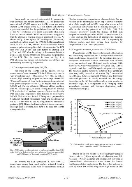
Ti: 50 nm<br />
Cr: 50 nm<br />
PZT film: 1 μm<br />
Pt/Ti: 200/50 nm<br />
SiO 2 : 2 μm<br />
Si: 500 μm<br />
Si: 400 μm<br />
4-inch<br />
11-13 <br />
May 2011, Aix-en-Provence, France<br />
<br />
Au film 100/300 nm<br />
Au film: 300 nm<br />
film low temperature integration on silicon substrate. We use<br />
Au film as the intermediate layer. Fig. 4 shows schematic<br />
view of the sample and its SAM image after bonded at 150<br />
°C. Die-shear test revealed that the bonding strength is ~75<br />
MPa at the bonding pressure of 325 MPa [16]. This<br />
technique effectively avoids the damage of PZT high<br />
temperature annealing to other MEMS components and ICs.<br />
It also enables the fabrication of piezoelectric material,<br />
piezoelectric MEMS components, and ICs separately by<br />
different wafers, and then bonded them together for<br />
integrated MEMS/ICs mass production.<br />
2.4 Energy dissipation in piezoelectric MEMS device<br />
Piezoelectric MEMS device offers great self-actuation<br />
and self-sensing capabilities, but it always suffers from low<br />
device performance in sensitivity. To investigate the energy<br />
dissipation mechanism, various cantilevers with different<br />
layers are designed and fabricated, which includes SiO 2<br />
elastic layer, Pt/Ti bottom electrode layer, PZT film, Ti/Pt/Ti<br />
upper electrode layer, and SiO 2 top electric passivation layer.<br />
The measured quality-factors (Q-factor) of those cantilevers<br />
were analyzed by theoretical calculation. Fig. 5 summarized<br />
the difference between measured Q-factors and theoretical<br />
calculated Q-factors. It clearly revealed that the energy<br />
dissipation by the PZT film and the multi-layered structure is<br />
extremely large. It is comparable to air dumping under<br />
atmospheric pressure and becomes dominating under<br />
reduced pressures [17].<br />
Q-factor decreases to calculated value (%)<br />
10<br />
0<br />
-10<br />
-20<br />
-30<br />
-40<br />
-50<br />
-60<br />
-70<br />
SiO 2<br />
SiO 2<br />
+Ti/Pt<br />
SiO 2<br />
+Ti/Pt+PZT+Ti/Pt/Ti+SiO 2<br />
SiO 2<br />
+Ti/Pt+PZT<br />
Length: 200 μm<br />
Length: 250 μm<br />
Length: 300 μm<br />
1 2 3 4 5<br />
Number of structure layer<br />
Fig.5 Q-factor of the cantilever decreased with the increasing of structure<br />
layers, especially after PZT film integration.<br />
Fig. 4 PZT bonding on silicon substrate by surface activated bonding (SAB)<br />
using Au film as the intermediate layer: schematic view of the sample (left)<br />
and SAM images of the sample bonded at 150 °C (right).<br />
To promote the PZT application in case >400 °C<br />
temperature cannot been used, surface activated bonding<br />
(SAB) was introduced in our work for the first time for PZT<br />
Based on above results, a piezoelectrically-actuated<br />
micro cantilever [18] and a piezoelectrically-transduced disk<br />
resonator [19] were designed and fabricated in our work as<br />
resonant-based ultra-sensitive mass sensor for human<br />
healthcare and other applications. The device fabrication was<br />
done by 4-inch SOI wafers using above large area PZT film<br />
219


