

Online proceedings - EDA Publishing Association
Online proceedings - EDA Publishing Association
Online proceedings - EDA Publishing Association

You also want an ePaper? Increase the reach of your titles
YUMPU automatically turns print PDFs into web optimized ePapers that Google loves.
al. used a modified LIGA (German acronym for LIthografie,<br />
Galvanoformung, and Abformung) process to fabricate<br />
microlenses by melting the deep x-ray irradiated pattern onto<br />
a PMMA (poly-methyl methacrylate) substrate. Using this<br />
technique, microoptical components of any desired shape can<br />
be fabricated [6, 7]. The resulting components have smooth<br />
and vertical sidewalls, lateral dimensions in the micrometer<br />
range, and sag heights of several hundred micrometers. A<br />
molding process (either injection molding or hot embossing)<br />
is required before mass production can be achieved. The<br />
microlens array mold or mold inserts play an important role in<br />
the mass molding production process. This replication<br />
process promises the desired profile as final products.<br />
A new method for producing microlens array with large<br />
sag heights was investigated for integrated fluorescence<br />
microfluidic detection systems [8]. Three steps in that<br />
production technique were included for concave microlens<br />
array formations to be integrated into microfluidic systems.<br />
The micro concave lens molds were then finished and ready<br />
to produce convex microlens in PDMS material. Using a<br />
LIGA-like process to fabricate microlens arrays is<br />
considerably less expensive using a UV exposure tool instead<br />
of deep x-ray lithography. A new microlens array fabrication<br />
method using a UV proximity printing method has been<br />
invented [9]. It uses a slice to control the gap size, resulting in<br />
microlens array formation in the resist. However, this method<br />
was limited to round microlens arrays with low sag heights.<br />
They produced microstructures with smooth surfaces, high<br />
yield rates, and good reliability.<br />
The LIGA-like process provides microlens array<br />
fabricators with high optical quality at low cost. By using the<br />
vacuum pressure to form a microlens array was investigated<br />
[10]. This vacuum suction technique is feasible for certain<br />
microlens array fabrication sizes. Based on the LIGA-like<br />
technology development, this paper will present the<br />
promising technique using the LIGA-like process to pressing<br />
microlens array and investigate the processing parameters for<br />
making microlens array.<br />
11-13 <br />
May 2011, Aix-en-Provence, France<br />
<br />
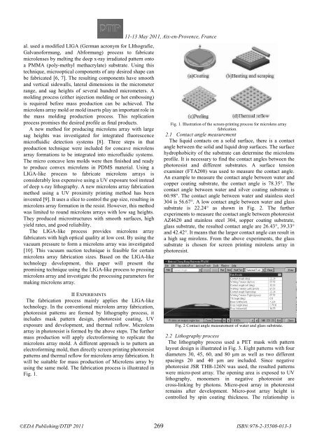
Fig. 1. Illustration of the screen-printing process for microlens array<br />
fabrication.<br />
2.1 Contact angle measurement<br />
The liquid contacts on a solid surface, there is a contact<br />
angle between the solid and liquid drop surfaces. The surface<br />
hydrophobicity of the substrate can determine the microlens<br />
profile. It is necessary to find the contact angles between the<br />
photoresist and different substrates. A surface tension<br />
examiner (FTA200) was used to measure the contact angle.<br />
An example to measure the contact angle between water and<br />
copper coating substrate, the contact angle is 78.35°. The<br />
contact angle between water and silver coating substrate is<br />
60.98°. The contact angle between water and stainless steel<br />
304 is 56.67°. A low contact angle between water and glass<br />
substrate is 22.24° as shown in Fig. 2. The further<br />
experiments to measure the contact angle between photoresist<br />
AZ4620 and stainless steel 304, sopper coating substrate,<br />
glass substrate, the resulted contact angle are 26.43°, 39.33°<br />
and 42.42°. It means that the larger contact angle can result in<br />
a high sag mirolens. From the above experiments, the glass<br />
substrate is chosen for screen printing mirolens array in<br />
photoresist.<br />
II EXPERIEMNTS<br />
The fabrication process mainly applies the LIGA-like<br />
technology. In the conventional microlens array fabrication,<br />
photoresist patterns are formed by lithography process, it<br />
includes mask pattern design, photoresist coating, UV<br />
exposure and development, and thermal reflow. Microlens<br />
array in photoresist is formed by the above steps. The further<br />
mass production will apply electroforming to replicate the<br />
microlens array mold. A different approach is to pattern an<br />
electroforming mold, then directly screen printing photoresist<br />
patterns and thermal reflow formicrolens array fabrication. It<br />
will be suitable for mass production of Microlens array by<br />
using the same mold. The fabrication process is illustrated in<br />
Fig. 1.<br />
Fig. 2 Contact angle measurement of water and glass substrate.<br />
2.2 Lithography process<br />
The lithography process used a PET mask with pattern<br />
layout design is illustrated in Fig. 3. Eight patterns with four<br />
diameters 30, 45, 60, and 80μm as well as two different<br />
spacings 20 and 40 μm are included. Since negative<br />
photoresist JSR THB-126N was used, the resulted patterns<br />
were micro-post array. The opening area is exposed to UV<br />
lithography, monomers in negative photoresist are<br />
cross-linking by photons. Micro-post array in photoresist<br />
remains after development. Micro-post array height is<br />
controlled by spin coating thickness. The relationship is<br />
269


