

Online proceedings - EDA Publishing Association
Online proceedings - EDA Publishing Association
Online proceedings - EDA Publishing Association

Create successful ePaper yourself
Turn your PDF publications into a flip-book with our unique Google optimized e-Paper software.
The fabrication of optical Cap-Wafers, i.e. the fabrication of<br />
cavity windows with high optical performance (Fig. 1b) on<br />
wafer-level processing, poses an extra challenge for<br />
manufacturing.<br />
Conventional methods forming a cavity are commonly using<br />
subtractive processes such as plasma etching, wet etching or<br />
even more coarse processes like sandblasting and ultrasound<br />
milling. These processes remove material from a wafer<br />
substrate (e.g. a polished glass wafer) in unmasked areas thus<br />
forming a cavity; whereas the material which is protected by a<br />
masking technology remains and forms bond frames or<br />
similar structures. It should be noted, that processing takes<br />
place in the bottom of the cavity,<br />
In case of an optical cavity this surface represents the optical<br />
active surface and is, especially with shallow cavities, very<br />
close to the focal plane of an optical sensor. Furthermore any<br />
optical surface finish in the cavity area such as highly<br />
polished surfaces, antireflective / filter coatings or optical<br />
elements like gratings and apertures are damaged by the<br />
cavity formation using subtractive processes.<br />
These drawbacks can be avoided by using additive techniques.<br />
In this case bond frames or similar structures are formed<br />
on top of a high quality optical wafer by depositing material<br />
whereas the optical area in the bottom of the cavity shall<br />
remain intact.<br />
Most commonly photoactive polymers are used to form the<br />
frames like BCB or SU-8. These materials are typically<br />
applied by spin- or spray-on, structured using lithography<br />
where the photosensitive material is selectively exposed and<br />
removed in a development step thus forming the bond frames<br />
very precisely. This method is the mainstream solution for<br />
low-end product, where the disadvantages of polymers like<br />
limited reliability, moisture uptake, oxygen or moisture<br />
transmission or degradation at elevated temperatures play a<br />
minor role.<br />
In the effort to meet reliability requirements for advanced<br />
products stencil printing of frit-glass or solder glasses is used.<br />
However these glass-powder based materials generate<br />
particles during processing and the resolution of the lateral<br />
dimensions as well as the height of the frames structures is<br />
limited by the minimal grain size of the glass-powder, the<br />
stencil printing process and the need for a reflow process for<br />
post-processing the glass-slurries.<br />
In order to overcome the limitations of todays mainstream<br />
solutions, we propose a novel method to fabricate precise and<br />
hermetic Cap-Wafers with high optical quality:<br />
Shallow Cavities using Additive Microstructuring of Glass<br />
– Lithoglas process<br />
An advanced, additive microstructuring process of glass<br />
(Lithoglas process) is used to fabricate a “glass-only” cap<br />
wafer providing utmost optical performance at a very low<br />
level of defects. The novel deposition and microstructuring of<br />
glass allows the formation of thin films of dense borosilicate<br />
glass on a broad range of substrates at substrate temperatures<br />
below 100 °C [3, 4].<br />
The deposition of the glass is done by a plasma-assisted e-<br />
beam evaporation process. It is a high rate deposition process<br />
11-13 May 2011, Aix-en-Provence, France<br />
<br />
<br />
with deposition rates of several hundred nm/min and at the<br />
same time low substrates temperature. With the high<br />
deposition rate typical film thicknesses of 3 – 20 µm can be<br />
achieved easily and production can be run as a cost effective<br />
batch process. Thicker layers as thick as 100 µm have been<br />
done in R&D – this is only possible due to the outstanding<br />
control of stress in the deposited layers.<br />
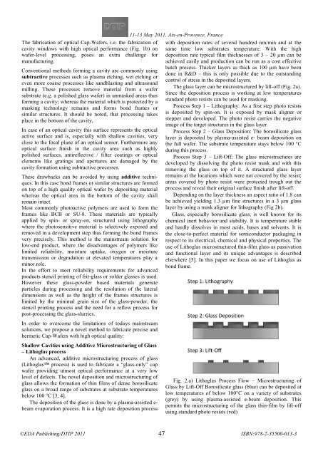
The glass layer can be microstructured by lift-off (Fig. 2a).<br />
Since the deposition process is working at low temperatures<br />
standard photo resists can be used for masking.<br />
Process Step 1 – Lithography: As a first step photo resists<br />
is deposited by spin-on. It is exposed by mask aligner or<br />
stepper and developed. The photo resist carries the negative<br />
image of the target structures in the glass layer.<br />
Process Step 2 – Glass Deposition: The borosilicate glass<br />
layer is deposited by plasma-assisted e- beam deposition on<br />
the full wafer. The substrate temperature stays below 100 °C<br />
during this process.<br />
Process Step 3 – Lift-Off: The glass microstructures are<br />
developed by dissolving the photo resist mask and with this<br />
removing the glass on top of it. A structured glass layer<br />
remains at the locations which were not covered by the resist;<br />
areas covered by photo resist were protected trough out the<br />
process and reveal their original surface finish after lift-off.<br />
Depending on the layer thickness an aspect ratio of 1.8 can<br />
be achieved yielding 1.3 µm fine structures in a 3 µm glass<br />
layer by using a mask aligner for lithography (Fig 2b).<br />
Glass, especially borosilicate glass, is well known for its<br />
chemical inert behavior and stability. It is temperature stable<br />
and hardly dissolves in most acids, bases and solvents. It is<br />
the close-to-perfect material for semiconductor packaging in<br />
respect to its electrical, chemical and physical properties. The<br />
use of Lithoglas microstructured thin-film glass as passivation<br />
and functional layer and its unique advantages is described<br />
elsewhere [5]. In this paper we focus on use of Lithoglas as<br />
bond frame.<br />
Fig. 2.a) Lithoglas Process Flow – Microstructuring of<br />
Glass by Lift-Off Borosilicate glass (blue) can be deposited at<br />
low temperatures of below 100°C on a variety of substrates<br />
(grey) by using plasma-assisted e-beam deposition. This<br />
permits the microstructuring of the glass thin-film by lift-off<br />
using standard photo resists (red)<br />
47


