

Online proceedings - EDA Publishing Association
Online proceedings - EDA Publishing Association
Online proceedings - EDA Publishing Association

You also want an ePaper? Increase the reach of your titles
YUMPU automatically turns print PDFs into web optimized ePapers that Google loves.
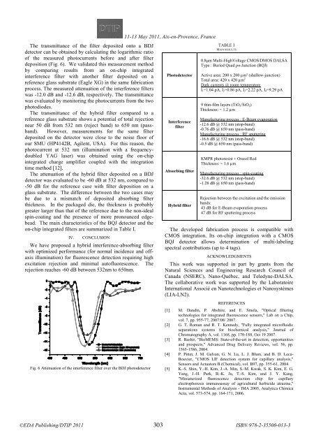
The transmittance of the filter deposited onto a BDJ<br />
detector can be obtained by calculating the logarithmic ratio<br />
of the measured photocurrents before and after filter<br />
deposition (Fig. 6). We validated this measurement method<br />
by comparing results from an on-chip integrated<br />
interference filter with another filter deposited on a<br />
reference glass substrate (Eagle XG) in the same fabrication<br />
process. The measured attenuation of the interference filters<br />
was -12.0 dB and -12.6 dB, respectively. The transmittance<br />
was evaluated by monitoring the photocurrents from the two<br />
photodiodes.<br />
The transmittance of the hybrid filter compared to a<br />
reference glass substrate shows a potential of total rejection<br />
near 50 dB from 532 nm (reject band) to 650 nm (passband).<br />
However, measurements for the same filter<br />
deposited on the detector were close to the noise floor of<br />
our SMU (HP4142B, Agilent, USA). For this reason, the<br />
photocurrent at 532 nm (illumination with a frequencydoubled<br />
YAG laser) was obtained using the on-chip<br />
integrated charge amplifier coupled with the integration<br />
time method [12].<br />
The attenuation of the hybrid filter deposited on a BDJ<br />
detector was evaluated to be -60 dB at 532 nm, compared to<br />
-50 dB for the reference case with filter deposition on a<br />
glass substrate. The difference between the two cases may<br />
be due to a mismatch of deposited absorbing filter<br />
thickness. In the packaged die, the thickness is probably<br />
greater larger than that of the reference due to the non-ideal<br />
spin-coating and the presence of more pronounced edgebead.<br />
The main characteristics of the BQJ detector and the<br />
on-chip integrated filters are summarized in Table I.<br />
IV. CONCLUSION<br />
We have proposed a hybrid interference-absorbing filter<br />
with optimized performance (for normal incidence and offaxis<br />
illumination) for fluorescence detection requiring high<br />
excitation rejection and minimal autofluorescence. The<br />
rejection reaches -60 dB between 532nm to 650nm.<br />
Fig. 6 Attenuation of the interference filter over the BDJ photodetector<br />
11-13 <br />
May 2011, Aix-en-Provence, France<br />
<br />
Photodetector<br />
Interference<br />
filter<br />
Absorbing filter<br />
Hybrid filter<br />
TABLE I<br />
MAIN RESULTS<br />
0.8μm Multi-HighVoltage CMOS/DMOS DALSA<br />
Type : Buried Quad pn-Junction (BQJ)<br />
Active area: 200 x 200 µm² (shallow-junction)<br />
Total area: 420 x 420 µm 2<br />
Dark currents @ room temperature<br />
I 1=1.04 pA, I 2=0.86 pA, I 3=2.22 pA, I 4=9.29 pA<br />
9 thin-film layers (TiO 2/SiO 2)<br />
Thickness: ~ 1.2 µm<br />
Manufacturing process : E-Beam evaporation<br />
-12.6 dB @ 532 nm (stop-band)<br />
-0.76 dB @ 650 nm (pass-band)<br />
Manufacturing process : RF sputtering<br />
-16.6 dB @ 532 nm (stop-band)<br />
-0.5 dB @ 650 nm (pass-band)<br />
KMPR photoresist + Orasol Red<br />
Thickness: ~ 1.6 µm<br />
Manufacturing process : spin-coating<br />
-32.6 dB @ 532 nm (stop-band)<br />
-1.28 dB @ 650 nm (pass-band)<br />
Rejection between the excitation and the emission<br />
bands:<br />
43 dB for E-Beam evaporation process<br />
47 dB for RF sputtering process<br />
The developed fabrication process is compatible with<br />
CMOS integration. Its on-chip integration with a CMOS<br />
BQJ detector allows determination of multi-labeling<br />
spectral contributions (up to 4 tags).<br />
ACKNOWLEDGMENTS<br />
This work was supported in part by grants from the<br />
Natural Sciences and Engineering Research Council of<br />
Canada (NSERC), Nano-Québec, and Teledyne-DALSA.<br />
The collaborative work was supported by the Laboratoire<br />
International Associé en Nanotechnologies et Nanosystèmes<br />
(LIA-LN2).<br />
REFERENCES<br />
[1] M. Dandin, P. Abshire, and E. Smela, "Optical filtering<br />
technologies for integrated fluorescence sensors," Lab on a Chip,<br />
vol. 7, pp. 955-77, 2007/08/ 2007.<br />
[2] G. T. Roman and R. T. Kennedy, "Fully integrated microfluidic<br />
separations systems for biochemical analysis," Journal of<br />
Chromatography A, vol. 1168, pp. 170-188, Oct 19 2007.<br />
[3] R. Bashir, "BioMEMS: State-of-the-art in detection, opportunities<br />
and prospects," Advanced Drug Delivery Reviews, vol. 56, pp.<br />
1565-1586, 2004.<br />
[4] P. Pittet, J. M. Galvan, G. N. Lu, L. J. Blum, and B. D. Leca-<br />
Bouvier, "CMOS LIF detection system for capillary analysis,"<br />
Sensors and Actuators B (Chemical), vol. B97, pp. 355-61, 2004.<br />
[5] K.-S. Shin, Y.-H. Kim, J.-A. Min, S.-M. Kwak, S. K. Kim, E. G.<br />
Yang, J.-H. Park, B.-K. Ju, T.-S. Kim, and J. Y. Kang,<br />
"Miniaturized fluorescence detection chip for capillary<br />
electrophoresis immunoassay of agricultural herbicide atrazine,"<br />
Instrumental Methods of Analysis - IMA 2005, Analytica Chimica<br />
Acta, vol. 573-574, pp. 164-171, 2006.<br />
303


