

Online proceedings - EDA Publishing Association
Online proceedings - EDA Publishing Association
Online proceedings - EDA Publishing Association

You also want an ePaper? Increase the reach of your titles
YUMPU automatically turns print PDFs into web optimized ePapers that Google loves.
11-13 <br />
May 2011, Aix-en-Provence, France<br />
photoresist for microlens array formation.<br />
<br />
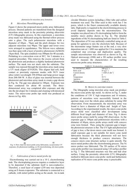
B. Microlens Photolithography<br />
Figure 4 shows the proposed micro probe array fabrication<br />
process. Desired patterns are transferred from the designed<br />
microlens array mask in the proximity printing ultraviolet<br />
(UV) lithographic process. In this experiment, a microlens<br />
array mask was fabricated using the thermal reflow process<br />
onto a glass. The each pohotoresist microlens with a<br />
diameter of 60μm , 70μm and the pitch distance for two<br />
adjacent microlens was 90μm. The upper and lower rows<br />
were arranged in equidistance. The Silicon wave substrate<br />
was then spun with a layer of positive photoresist (AZ4620)<br />
18μm thick. The spin condition was 500rpm for 40 seconds.<br />
Prebaking in a convection oven at 90℃<br />
for 3 minutes is a<br />
required procedure. This removes the excess solvent from<br />
the photoresist and produces a slightly hardened photoresist<br />
surface. The mask was not stuck onto the substrate. The<br />
sample was exposed through the microlens array mask using<br />
a UV mask aligner (EVG620). This aligner had soft, hard<br />
contact or proximity exposure modes with NUV (near<br />
ultra-violet) wavelength 350-450nm and lamp power range<br />
from 200-500 W. A slice of glass was inserted between the<br />
photoresist and microlens array mask to create a gap shown<br />
in Fig. 4a. The gap was adjusted to 100μm. Exposure was<br />
then conducted for about 40 seconds. The threedimensional<br />
array was completed after exposure and dip<br />
into the developer for 2 minutes and cleaning with deionized<br />
water. The micro-cone probe tips mold was produced as<br />
shown in Fig. 4(b).<br />
Fig. 4. Flow chart for micro probe array fabrication, (a) proximity UV<br />
exposure, (b) photoresist molding, (c) Ni electroforming, (d) micro probe<br />
array peel-off.<br />
C. Fabrication of micro metal probe tip<br />
Electroforming was carried out in a 10 L electroforming<br />
tank. The electroplating process requires a conductive layer<br />
to be deposited if the substrate itself is non-conductive.<br />
Therefore, a seed layer of copper (250 nm) was deposited<br />
usinganE-beam evaporator. The substrate is connected to a<br />
cathode, with nickel pellets acting as the anode. An in-tank<br />
circular filtration system including a filter tube and carbon<br />
treatment was used. The filter used in this work has 5 lm<br />
pores, which is the finest commercially available density<br />
tube. High purity is required in the electroforming process to<br />
avoid impurity deposits onto the microstructures. The<br />
template was placed into a Ni electroplating bath to form the<br />
metallic micro probes shown in Fig. 4c. The detailed<br />
ingredients of the Ni electroplating bath are listed in Table I.<br />
The deposition of Ni was uniformly controlled using an air<br />
pump for agitation to mix the electrolyte bath. Because of<br />
the micrometer range feature size at the end, a very slow<br />
deposition rate at 1 ASD was applied for 2 h to maintain the<br />
completed step coverage and duplication quality. The<br />
sample microstructure was observed as shown in Fig. 4d.<br />
Optical microscopy (OM) and a 3D surface profiler were<br />
used to measure the characteristics of the resulting<br />
microcone probe array structures.<br />
TABLE I Ni electrolyte composition<br />
Ni (NH2SO3)2_4H2O 500 (g L -1 )<br />
Boric acid 45(gL -1 )<br />
Current density 1 ASD (A dm -2 )<br />
pH 4<br />
Temperature 50 °C<br />
Agitation<br />
Air pump<br />
Wetting agent 3 (mL L -1 )<br />
Ⅳ. RESULTS AND DISCUSSION<br />
The lithography using microlen array mask can produce<br />
the micro-cone probe tips mold. As shown in Fig. 5, under<br />
the conditions of 150 °C high temperature and 10 minutes,<br />
patterns of microlens were successfully formed in the<br />
aperture stops over the whole glass substrate by using OM<br />
observation. From measurement, the microlens array was<br />
found to have a diameter of 60μm and height of 5μm.<br />
According to the experimental results, the micro cone probe<br />
arrays mold were classified after development using<br />
different focal length and diameter of lens. Fig. 6 shows<br />
micro probe arrays mold by using OM observation. As the<br />
exposure gap is 100μm and pohotoresist microlens with a<br />
diameter of 60μm, micro probe arrays mold with concave<br />
cone were formed. Then, using the exposure gap is larger;<br />
the photoresist structure is flat. The UV light and photoresist<br />
of gap is less; a flat down micro cone mold was formed. A<br />
small exposure gap is not suitable for micro cone mold<br />
fabrication because the thick photoresist will not have<br />
enough thickness to produce concave structures. The<br />
concave micro cone structure surface is quite smooth. The<br />
micro metal probes after the electroforming process. The Ni<br />
micro probes was fabricated. The 3D surface of Ni micro<br />
cone probe profiler was measured using 3-D surface profiler<br />
in Fig. 7. The fabricated structure was fine and had clear<br />
surface. Using the proximity ultraviolet (UV) lithography<br />
methodtofabricate micro cone probe mold and furthermore<br />
replication of Ni micro cone probe array is practicable.<br />
178


