- Page 4:
Musical Applications of Microproces
- Page 7 and 8:
© 19B5 by Hayden Books A Division
- Page 9 and 10:
serve to acquaint the general reade
- Page 11 and 12:
SECfrON II. Computer-Controlled Ana
- Page 13 and 14:
17. Digital Hardware 589 AnalogModu
- Page 16 and 17:
1 Music Synthesis Principles Creati
- Page 18 and 19:
MUSIC SYNTHESIS PRINCIPLES 5 own ar
- Page 20 and 21:
MusIC SYNTHESIS PRINCIPLES 7 Increa
- Page 22 and 23:
MUSIC SYNTHESIS PRINGPLES 9 VERY SM
- Page 24 and 25:
MUSIC SYNTHESIS PRINOPLES 11 repres
- Page 26 and 27:
MUSIC SYNTHESIS PRINCIPLES 13 The w
- Page 28 and 29:
MUSIC SYNTHESIS PRlNCIPLES 15 was c
- Page 30 and 31:
MUSIC SYNTHESIS PRlNOPlES 17 In act
- Page 32 and 33:
MUSIC SYNTHESIS PRINCIPLES 19 SIN (
- Page 34 and 35:
MUSIC SYNTHESIS PRINCIPLES 21 lILt!
- Page 36 and 37:
MUSIC SYNTHESIS PRINCIPLES 23 - ,--
- Page 38 and 39:
MUSIC SYNTHESIS PRINOPLES 25 + or--
- Page 40 and 41:
MUSIC SYNTHESIS PRINCIPLES 27 Human
- Page 42 and 43:
MUSIC SYNTHESIS PRINOPLES 29 fundam
- Page 44 and 45:
MUSIC SYNTHESIS PRINCIPLES 31 frequ
- Page 46 and 47:
MUSIC SYNTHESIS PRINCIPLES 33 from
- Page 48 and 49:
MUSIC SYNTHESIS PRINCIPLES 35 ever,
- Page 50 and 51:
MUSIC SYNTHESIS PRINCIPLES 37 have
- Page 52 and 53:
MUSIC SYNTHESIS PRINCIPLES 39 No li
- Page 54:
MUSIC SYNTHESIS PRINCIPLES 41 cropr
- Page 57 and 58:
44 MUSICAL ApPLICATIONS OF MICROPRO
- Page 59 and 60:
46 MUSICAL ApPLICATIONS OF MICROPRO
- Page 61 and 62:
48 MUSICAL ApPLICATIONS OF MICROPRO
- Page 63 and 64:
50 MUSICAL ApPLICATIONS OF MICROPRO
- Page 65 and 66:
52 MUSICAL ApPLICATIONS OF MICROPRO
- Page 67 and 68:
54 MUSICAL ApPLICATIONS OF MICROPRO
- Page 69 and 70:
56 MUSICAL ApPLICATIONS OF MICROPRO
- Page 71 and 72:
58 MUSICAL ApPLICATIONS OF MICROPRO
- Page 73 and 74:
60 MUSICAL ApPLICATrONS OF MICROPRO
- Page 75 and 76:
62 MUSICAL ApPLICATIONS OF MICROPRO
- Page 77 and 78:
64 MUSICAL ApPLICATIONS OF MICROPRO
- Page 79 and 80:
66 MUSICAL ApPLICATIONS OF MICROPRO
- Page 81 and 82:
68 MUSICAL ApPLICAnONS OF MICROPROC
- Page 83 and 84:
70 MUSICAL ApPLICAnONS OF MICROPROC
- Page 85 and 86:
72 MUSICAL ApPLICATIONS OF MICROPRO
- Page 87 and 88:
74 MUSICAL ApPLICAnONS OF MICROPROC
- Page 89 and 90:
76 MUSICAL ApPLICATIONS OF MICROPRO
- Page 91 and 92:
78 MUSICAL ApPLICATIONS OF MICROPRO
- Page 93 and 94:
80 MUSICAL ApPLICATIONS OF MICROPRO
- Page 95 and 96:
82 MUSICAL ApPUCATIONS OF MICROPROC
- Page 97 and 98:
84 MUSICAL ApPUCATIONS OF MICROPROC
- Page 99 and 100:
vvv·(B) 86 MUSICAL ApPLICATIONS OF
- Page 101 and 102:
88 MUSICAL ApPLICATIONS OF MICROPRO
- Page 103 and 104:
90 MUSICAL ApPLICATIONS OF MICROPRO
- Page 105 and 106:
92 MUSICAL ApPLICATIONS OF MICROPRO
- Page 107 and 108:
94 MUSICAL ApPLICATIONS OF MICROPRO
- Page 109 and 110:
96 MUSICAL ApPLICATIONS OF MICROPRO
- Page 111 and 112:
98 MUSICAL ApPLICATIONS OF MICROPRO
- Page 113 and 114:
100 MUSICAL ApPLICAnONS OF MICROPRO
- Page 115 and 116:
102 MUSICAL ApPLICATIONS OF MICROPR
- Page 117 and 118:
104 MUSICAL ApPLICATIONS OF MICROPR
- Page 119 and 120:
106 MUSICAL ApPLICATIONS OF MICROPR
- Page 121 and 122:
108 MUSICAL ApPLICATIONS OF MICROPR
- Page 123 and 124:
110 MUSICAL ApPLICATIONS OF MICROPR
- Page 125 and 126:
112 MUSICAL ApPLICATIONS OF MICROPR
- Page 127 and 128:
114 MUSICAL ApPLICATIONS OF MICROPR
- Page 129 and 130:
116 MUSICAL ApPLICATIONS OF MICROPR
- Page 131 and 132:
118 MUSICAL ApPLICATIONS OF MICROPR
- Page 133 and 134:
120 MUSICAL ApPLICATIONS OF MICROPR
- Page 135 and 136:
122 MUSICAL ApPLICATIONS OF MICROPR
- Page 137 and 138:
124 MUSICAL ApPLICATIONS OF MICROPR
- Page 139 and 140:
126 MUSICAL ApPLICATIONS OF MICROPR
- Page 141 and 142:
128 MUSICAL ApPLICATIONS OF MICROPR
- Page 143 and 144:
130 MUSICAL ApPLICATIONS OF MICROPR
- Page 145 and 146:
132 MUSICAL ApPLICATIONS OF MICROPR
- Page 147 and 148:
134 MUSICAL ApPLICATIONS OF MICROPR
- Page 149 and 150:
136 MUSICAL ApPLICATIONS OF MICROPR
- Page 151 and 152:
138 MUSICAL ApPLICATIONS OF MICROPR
- Page 153 and 154:
140 MUSICAL ApPLICATIONS OF MICROPR
- Page 155 and 156:
142 MUSICAL ApPLICATIONS OF MICROPR
- Page 157 and 158:
144 MUSICAL ApPLICATIONS OF MICROPR
- Page 159 and 160:
146 MUSICAL ApPLICATIONS OF MICROPR
- Page 161 and 162:
148 MUSICAL ApPLICATIONS OF MICROPR
- Page 163 and 164:
150 MUSICAL ApPLICATIONS OF MICROPR
- Page 165 and 166:
152 MUSICAL ApPLICATIONS OF MICROPR
- Page 167 and 168:
154 MUSICAL ApPLICATIONS OF MICROPR
- Page 169 and 170:
156 MUSICAL ApPLICATIONS OF MICROPR
- Page 171 and 172:
Table 5-1. 6502 Instruction Set Lis
- Page 173 and 174:
160 MUSICAL ApPLICATIONS OF MICROPR
- Page 175 and 176:
162 MUSICAL ApPLICATIONS OF MICROPR
- Page 177 and 178:
164 MUSICAL ApPLICATIONS OF MICROPR
- Page 179 and 180:
166 MUSICAL ApPLICATIONS OF MICROPR
- Page 181 and 182:
Coding Table 5-3. 68000 Addressing
- Page 183 and 184:
Table 5-4. 68000 Instruction Set Su
- Page 185 and 186:
Table 5-4. 68000 Instruction Set Su
- Page 187 and 188:
174 MUSICAL ApPLICATIONS OF MICROPR
- Page 190 and 191:
6 BasicAnalogModules Probably the m
- Page 192 and 193:
BASIC ANALOG MODULES 179 tage remai
- Page 194 and 195:
BASIC ANALOG MODULES 181 Op-amps ma
- Page 196 and 197:
BASIC ANALOG MODULES 183 '0: :? u
- Page 198 and 199:
BASIC ANALOG MODULES 185 with an id
- Page 200 and 201:
BASIC ANALOG MODULES 187 EXPONENTIA
- Page 202 and 203:
BASIC ANALOG MODULES 189 (or 0.9766
- Page 204 and 205:
BASIC ANALOG MODULES 191 4R Vr'o'M
- Page 206 and 207:
BASIC ANALOG MODULES 193 tooth with
- Page 208 and 209:
BASIC ANALOG MODULES 195 +IOVrel PU
- Page 210 and 211:
BASIC ANALOG MODULES 197 Table 6-1.
- Page 212 and 213:
BASIC ANALOG MODULES 199 constants
- Page 214 and 215:
BASIC ANALOG MODULES 201 12 ~ E 1-
- Page 216 and 217:
BASIC ANALOG MODULES 203 R2 R3 100
- Page 218 and 219:
BASIC ANALOG MODULES 205 fore, must
- Page 220 and 221:
BASIC ANALOG MODULES 207 For peak p
- Page 222 and 223:
BASIC ANALOG MODULES 209 22 pF RI S
- Page 224 and 225:
BASIC ANALOG MODULES 211 INPUT~OUTP
- Page 226 and 227:
BASIC ANALOG MODULES 213 Voltage-Tu
- Page 228 and 229:
BASIC ANALOG MODULES 215 +20 +15 +1
- Page 230 and 231:
BASIC ANALOG MODULES 217 100 ko. BA
- Page 232 and 233:
BASIC ANALOG MODULES 219 +15 V0----
- Page 234 and 235:
Digital-to-Analog and tlnalog-to-Di
- Page 236 and 237:
DIGITAL-TO-ANALOG AND ANALOG-TO-DIG
- Page 238 and 239:
DIGITAL-TO-ANALOG AND ANALOG-TO-DIG
- Page 240 and 241:
DIGITAL-TO-ANALOG AND ANALOG-TO-DIG
- Page 242 and 243:
DIGITAL-TO-ANALOG AND ANALOG-TO-DIG
- Page 244 and 245:
DIGITAL-TO-ANALOG AND ANALOG-TO-DIG
- Page 246 and 247:
DIGITAL-TO-ANALOG AND ANALOG-TO-DIG
- Page 248 and 249:
DIGITAL-TO-ANALOG AND ANALOG-TO-DIG
- Page 250 and 251:
DIGITAL-TO-ANALOG AND ANALOG-TO-DIG
- Page 252 and 253:
DIGITAL-TO-ANALOG AND ANALOG-TO-DIG
- Page 254 and 255:
DIGITAL-TO-ANALOG AND ANALOG-TO-DIG
- Page 256 and 257:
DIGITAL-TO-ANALOG AND ANALOG-TO-DIG
- Page 258 and 259:
DIGITAL-TO-ANALOG AND ANALOG-TO-DIG
- Page 260 and 261:
DIGITAL-TO-ANALOG AND ANALOG-TO-DIG
- Page 262 and 263:
DIGITAL-TO-ANALOG AND ANALOG-TO-DIG
- Page 264 and 265:
DIGITAL-TO-ANALOG AND ANALOG-TO-DIG
- Page 266 and 267:
DIGITAL-TO-ANALOG AND ANALOG-TO-DIG
- Page 268 and 269:
DIGITAL-TO-ANALOG AND ANALOG-TO-DIG
- Page 270 and 271:
DIGITAL-TO-ANALOG AND ANALOG-TO-DIG
- Page 272 and 273:
DIGITAL-TO-ANALOG AND ANALOG-TO-DIG
- Page 274 and 275:
DIGITAL-TO-ANALOG AND ANALOG-TO-DIG
- Page 276 and 277:
DIGITAL-TO-ANALOG AND ANALOG-TO-DIG
- Page 278 and 279:
DIGITAL-TO-ANALOG AND ANALOG-TO-DIG
- Page 280 and 281:
DIGITAL-TO-ANALOG AND ANALOG-TO-DIG
- Page 282:
DIGITAL-TO-ANALOG AND ANALOG-TO-DIG
- Page 285 and 286:
272 MUSICAL ApPLICATIONS OF MICROPR
- Page 287 and 288:
274 MUSICAL ApPLICATIONS OF MICROPR
- Page 289 and 290:
276 MUSICAL ApPLICATIONS OF MICROPR
- Page 291 and 292:
278 MUSICAL ApPLICATIONS OF MICROPR
- Page 293 and 294:
280 MUSICAL ApPLICATIONS OF MICROPR
- Page 295 and 296:
282 MUSICAL ApPLICATIONS OF MICROPR
- Page 297 and 298:
284 MUSICAL ApPLICATIONS OF MICROPR
- Page 299 and 300:
286 MUSICAL ApPLICATIONS OF MICROPR
- Page 301 and 302:
288 MUSICAL ApPLICATIONS OF MICROPR
- Page 303 and 304:
290 MUSICAL ApPLICATIONS OF MICROPR
- Page 305 and 306:
292 MUSICAL ApPLICATIONS OF MICROPR
- Page 307 and 308:
294 MUSICAL ApPLICATIONS OF MICROPR
- Page 309 and 310:
296 MUSICAL ApPLICATIONS OF MICROPR
- Page 311 and 312:
298 MUSICAL ApPLICATIONS OF MICROPR
- Page 313 and 314:
300 MUSICAl ApPLICATIONS OF MICROPR
- Page 315 and 316:
302 MUSICAL ApPLICATIONS OF MICROPR
- Page 317 and 318:
304 MUSICAL ApPLICATIONS OF MICROPR
- Page 319 and 320:
306 MUSICAL ApPLICATIONS OF MICROPR
- Page 321 and 322:
308 MUSICAL ApPLICATIONS OF MICROPR
- Page 323 and 324:
310 MUSICAL ApPLICATIONS OF MICROPR
- Page 325 and 326:
312 MUSICAL ApPLICATIONS OF MICROPR
- Page 327 and 328:
314 MUSICAL ApPLICATIONS OF MICROPR
- Page 329 and 330:
316 MUSICAL ApPLICATIONS OF MICROPR
- Page 331 and 332:
318 MUSICAL ApPLICATIONS OF MICROPR
- Page 333 and 334:
320 MUSICAL ApPLICATIONS OF MICROPR
- Page 335 and 336:
322 MUSICAL ApPLICATIONS OF MICROPR
- Page 337 and 338:
324 MUSICAL ApPLICATIONS OF MICROPR
- Page 339 and 340:
326 MUSICAL ApPLICATIONS OF MICROPR
- Page 341 and 342:
328 MUSICAL ApPLICATIONS OF MICROPR
- Page 343 and 344:
330 MUSICAL ApPLICATIONS OF MICROPR
- Page 345 and 346:
332 MUSICAL ApPLICATIONS OF MICROPR
- Page 347 and 348:
334 MUSICAL ApPLICATIONS OF MICROPR
- Page 349 and 350:
336 MUSICAL ApPLICATIONS OF MICROPR
- Page 352 and 353:
11 CORtrolSequeRce Display andEditi
- Page 354 and 355:
CONTROL SEQUENCE DISPLAY AND EDITIN
- Page 356 and 357:
CONTROL SEQUENCE DISPLAY AND EDITIN
- Page 358 and 359:
CONTROL SEQUENCE DISPLAY AND EDITIN
- Page 360 and 361:
CONTROL SEQUENCE DISPLAY AND EDITIN
- Page 362 and 363:
CONTROL SEQUENCE DISPLAY AND EDITIN
- Page 364 and 365:
CONTROL SEQUENCE DISPLAY AND EDITIN
- Page 366 and 367:
CONTROL SEQUENCE DISPLAY AND EDITIN
- Page 368 and 369:
CONTROL SEQUENCE DISPLAY AND EDITIN
- Page 370 and 371:
CONTROL SEQUENCE DISPLAY AND EDITIN
- Page 372 and 373:
CONTROL SEQUENCE DISPLAY AND EDITIN
- Page 374 and 375:
CONTROL SEQUENCE DISPLAY AND EDITIN
- Page 376 and 377:
CONTROL SEQUENCE DISPLAY AND EDITIN
- Page 378:
SECTIONIII DigitalSynthesis antl So
- Page 381 and 382:
368 MUSICAL ApPLICATIONS OF MICROPR
- Page 383 and 384:
370 MUSICAL ApPLICATIONS OF MICROPR
- Page 385 and 386:
372 MUSICAL ApPLICATIONS OF MICROPR
- Page 387 and 388:
374 MUSICAL ApPLICATIONS OF MICROPR
- Page 389 and 390:
376 MUSICAL ApPLICATIONS OF MICROPR
- Page 391 and 392:
378 MUSICAL ApPLICATIONS OF MICROPR
- Page 393 and 394:
380 MUSICAL ApPLICATIONS OF MICROPR
- Page 395 and 396:
382 MUSICAL ApPLICATIONS OF MICROPR
- Page 397 and 398:
384 MUSICAL ApPLICATIONS OF MICROPR
- Page 399 and 400:
386 MUSICAL ApPLICATIONS OF MICROPR
- Page 401 and 402:
388 MUSICAL ApPLICATIONS OF MICROPR
- Page 403 and 404:
390 MUSICAL ApPLICATIONS OF MICROPR
- Page 405 and 406:
392 MUSICAL ApPLICATIONS OF MICROPR
- Page 407 and 408:
394 MUSICAL ApPLICATIONS OF MICROPR
- Page 409 and 410:
396 MUSICAL ApPLICATIONS OF MICROPR
- Page 411 and 412:
Table 12·1. Design Data for Chebys
- Page 413 and 414:
~ o Table 12·1. (Cont.) Ripple = 1
- Page 415 and 416:
402 MUSICAL ApPLICATIONS OF MICROPR
- Page 417 and 418:
404 MUSICAL ApPLICATIONS OF MICROPR
- Page 419 and 420:
406 MUSICAL ApPLICATIONS OF MICROPR
- Page 421 and 422:
408 MUSICAL ApPLICATIONS OF MICROPR
- Page 423 and 424:
410 MUSICAL ApPLICATIONS OF MICROPR
- Page 425 and 426:
412 MUSICAL ApPLICATIONS OF MICROPR
- Page 427 and 428:
414 MUSICAL ApPLICATIONS OF MICROPR
- Page 430 and 431:
13 Digital Tone Generation Teehniqu
- Page 432 and 433:
DIGITAL TONE GENERATION TECHNIQUES
- Page 434 and 435:
DIGITAL TONE GENERATION TECHNIQUES
- Page 436 and 437:
DIGITAL TONE GENERATION TECHNIQUES
- Page 438 and 439:
DIGITAL TONE GENERATION TECHNIQUES
- Page 440 and 441:
DIGITAL TONE GENERATION TECHNIQUES
- Page 442 and 443:
DIGITAL TONE GENERATION TECHNIQUES
- Page 444 and 445:
DIGITAL TONE GENERATION TECHNIQUES
- Page 446 and 447:
DIGITAL TONE GENERATION TECHNIQUES
- Page 448 and 449:
DIGITAL TONE GENERATION TECHNIQUES
- Page 450 and 451:
DIGITAL TONE GENERATION TECHNIQUES
- Page 452 and 453:
DIGITAL TONE GENERATION TECHNIQUES
- Page 454 and 455:
DIGITAL TONE GENERATION TECHNIQUES
- Page 456 and 457:
Sample Number Harm. No. o 2 3 4 5 6
- Page 458 and 459:
Sample Spectrum Number 0 1 2 3 4 5
- Page 460 and 461:
DIGITAL TONE GENERATION TECHNIQUES
- Page 462 and 463:
DIGITAL TONE GENERATION TECHNIQUES
- Page 464 and 465:
DIGITAL TONE GENERATION TECHNIQUES
- Page 466 and 467:
DIGITAL TONE GENERATION TECHNIQUES
- Page 468 and 469:
DIGITAL TONE GENERATION TECHNIQUES
- Page 470 and 471:
DIGITAL TONE GENERATION TECHNIQUES
- Page 472 and 473:
DIGITAL TONE GENERATION TECHNIQUES
- Page 474 and 475:
DIGITAL TONE GENERATION TECHNIQUES
- Page 476 and 477:
DIGITAL TONE GENERATION TECHNIQUES
- Page 478 and 479:
DIGITAL TONE GENERATION TECHNIQUES
- Page 480 and 481:
DIGITAL TONE GENERATION TECHNIQUES
- Page 482 and 483:
1,0 0,8 0,6 0.4 0,2 °0 10 12 14 16
- Page 484 and 485:
DIGITAL TONE GENERATION TECHNIQUES
- Page 486 and 487:
DIGITAL TONE GENERATION TECHNIQUES
- Page 488 and 489:
1,o,-----------,----------" Y Ol---
- Page 490 and 491:
DIGITAL TONE GENERATION TECHNIQUES
- Page 492 and 493:
DIGITAL TONE GENERATION TECHNIQUES
- Page 494 and 495:
14 DigitalFiltering In analog synth
- Page 496 and 497:
DIGITAL FILTERING 483 Input Samples
- Page 498 and 499:
DIGITAL FILTERING 485 the input wav
- Page 500 and 501:
DIGITAL FILTERING 487 where 0 is no
- Page 502 and 503:
DIGITAL FILTERING 489 BAND REJECT >
- Page 504 and 505:
DIGITAL FILTERING 491 Next the inpu
- Page 506 and 507:
DIGITAL. FILTERING 493 circuits mak
- Page 508 and 509:
DIGITAL FILTERING 495 OUTPUT Fig. 1
- Page 510 and 511:
DIGITAL FILTERING 497 INPUT ~8~~~~~
- Page 512 and 513:
DIGITAL FILTERING 499 the turnover
- Page 514 and 515:
DIGITAL FILTERING 501 frequency is
- Page 516 and 517:
+ 3 1 oL-_-...l__---l__---L__---r-_
- Page 518 and 519:
DIGITAL FILTERING 505 When programm
- Page 520 and 521:
DIGITAL FILTERING 507 lowest freque
- Page 522 and 523:
DIGITAL FILTERING 509 Even with a p
- Page 524 and 525:
DIGITAL FILTERING 511 OUTPUT Fig. 1
- Page 526 and 527:
DIGITAL FILTERING 513 INPUT VARIABL
- Page 528 and 529:
DIGITAL FILTERING 515 INPUT (C) -(.
- Page 530 and 531:
DIGITAL FILTERING 517 NOTE: Xl, Y,
- Page 532 and 533:
DIGITAL FILTERING 519 AMPLITUDE, (d
- Page 534 and 535:
DIGITAL FILTERING 521 o ~ -10 ~ -20
- Page 536 and 537:
DIGITAL FILTERING 523 1.0 0.8 0.6
- Page 538:
DIGITAL FILTERING 525 When the outp
- Page 541 and 542:
528 MUSICAL ApPLICATIONS OF MICROPR
- Page 543 and 544:
530 MUSICAL ApPLICATIONS OF MICROPR
- Page 545 and 546:
532 MUSICAL ApPLICATIONS OF MICROPR
- Page 547 and 548:
534 MUSICAL ApPLICATIONS OF MICROPR
- Page 549 and 550:
536 MUSICAL ApPLICATIONS OF MICROPR
- Page 551 and 552:
538 MUSICAL ApPLICATIONS OF MICROPR
- Page 553 and 554:
540 MUSICAL ApPLICATIONS OF MICROPR
- Page 556 and 557:
16 Source-SignalAnalys,is One of th
- Page 558 and 559:
SOURCE-SIGNAL ANALYSIS 545 nOdB T I
- Page 560 and 561:
--------, I I ! II i I I I I , , i"
- Page 562 and 563:
SOURCE-SIGNAL ANALYSIS 549 3 IN -"
- Page 564 and 565:
SOURCE-SIGNAL ANALYSIS 551 Data Rep
- Page 566 and 567:
SOURCE-SIGNAL ANALYSIS 553 SIGNAL B
- Page 568 and 569:
SOURCE-SIGNAL ANALYSIS 555 -5° FH
- Page 570 and 571: SOURCE-SIGNAL ANALYSIS 557 -5 -10 ~
- Page 572 and 573: SOURCE-SIGNAL ANALYSIS 559 Since th
- Page 574 and 575: SOURCE-SIGNAL ANALYSIS 561 o -5 -10
- Page 576 and 577: SOURCE-SIGNAL ANALYSIS 563 o -5 -10
- Page 578 and 579: SOURCE-SIGNAL ANALYSIS 565 overlapp
- Page 580 and 581: SOURCE-SIGNAL ANALYSIS 567 • ....
- Page 582 and 583: SOURCE-SIGNAL ANALYSIS 569 from an
- Page 584 and 585: SOURCE-SIGNAL ANALYSIS 571 componen
- Page 586 and 587: SOURCE-SIGNAL ANALYSIS 573 and some
- Page 588 and 589: SOURCE-SIGNAL ANALYSIS 575 185491 A
- Page 590 and 591: SOURCE-SIGNAL ANALYSIS 577 SYSTEM F
- Page 592 and 593: SOURCE-SIGNAL ANALYSIS 579 (AI (BI
- Page 594 and 595: SOURCE-SIGNAL ANALYSIS 581 (Gl II'
- Page 596 and 597: SOURCE-SIGNAL ANALYSIS 583 PULSE PE
- Page 598 and 599: SOURCE-SIGNAL ANALYSIS 585 again, t
- Page 600 and 601: SOURCE-SIGNAL ANALYSIS 587 Quite ob
- Page 602 and 603: 17 DigitalHardware At this point, w
- Page 604 and 605: DIGITAL HARDWARE 591 Lsa I N+I DIVI
- Page 606 and 607: DIGITAL HARDWARE 593 (~OCK[ L _ LSB
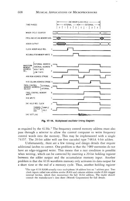
- Page 608 and 609: DIGITAL HARDWARE 595 FREQUENCY CONT
- Page 610 and 611: DIGITAL HARDWARE 597 Fig. 17-7. Pha
- Page 612 and 613: DIGITAL HARDWARE 599 MOST SIGNIFICA
- Page 614 and 615: DIGITAL HARDWARE 601 waveform chang
- Page 616 and 617: DIGITAL HARDWARE 603 As an example,
- Page 618 and 619: DIGITAL HARDWARE 605 1. Sixteen ind
- Page 622 and 623: DIGITAL HARDWARE 609 between the 41
- Page 624 and 625: DIGITAL HARDWARE 611 8-BIT PORT I M
- Page 626 and 627: FREOUENCY CONTROL IN I I 20 FREOUEN
- Page 628 and 629: DIGITAL HARDWARE 615 TO MULTIPLEXED
- Page 630 and 631: FREQ. :a.-8 CNTL. WRITE FREQ. I 20
- Page 632 and 633: DIGITAL HARDWARE 619 effective freq
- Page 634 and 635: DIGITAL HARDWARE 621 The signal mem
- Page 636 and 637: DIGITAL HARDWARE 623 into a filter
- Page 638 and 639: DIGITAL HARDWARE 625 made using con
- Page 640 and 641: DIGITAL HARDWARE 627 A Hybrid Voice
- Page 642 and 643: DIGITAL HARDWARE 629 o -5 -10 -15 ~
- Page 644 and 645: DIGITAL HARDWARE 631 o -5 -10 -15 ~
- Page 646 and 647: DIGITAL HARDWARE 633 D3 02 01 10 00
- Page 648 and 649: DIGITAL HARDWARE 635 plementers on
- Page 650: DIGITAL HARDWARE 637 taken care of
- Page 653 and 654: 640 MUSICAL ApPLICATIONS OF MICROPR
- Page 655 and 656: 642 MUSICAL ApPLICATIONS OF MICROPR
- Page 657 and 658: 644 MUSICAL ApPLICATIONS OF MICROPR
- Page 659 and 660: 646 MUSICAL ApPLICATIONS OF MICROPR
- Page 661 and 662: 648 MUSICAL ApPLICATIONS OF MICROPR
- Page 663 and 664: 650 MUSICAL ApPLICATIONS OF MICROPR
- Page 665 and 666: 652 MUSICAL ApPLICATIONS OF MICROPR
- Page 667 and 668: 654 MUSICAL ApPLICATIONS OF MICROPR
- Page 669 and 670: 656 MUSICAL ApPLICATIONS OF MICROPR
- Page 671 and 672:
658 MUSICAL ApPLICATIONS OF MICROPR
- Page 673 and 674:
660 MUSICAL ApPLICATIONS OF MICROPR
- Page 675 and 676:
662 MUSICAL ApPLICATIONS OF MICROPR
- Page 677 and 678:
664 MUSICAL ApPLICATIONS OF MICROPR
- Page 679 and 680:
666 MUSICAL ApPLICATIONS OF MICROPR
- Page 681 and 682:
668 MUSICAL ApPLICATIONS OF MICROPR
- Page 683 and 684:
670 MUSICAL ApPLICATIONS OF MICROPR
- Page 685 and 686:
672 MUSICAL ApPLICATIONS OF MICROPR
- Page 687 and 688:
674 MUSICAL ApPLICATIONS OF MICROPR
- Page 689 and 690:
676 MUSICAL ApPLICATIONS OF MICROPR
- Page 691 and 692:
678 MUSICAL ApPLICATIONS OF MICROPR
- Page 693 and 694:
680 MUSICAL ApPLICATIONS OF MICROPR
- Page 695 and 696:
682 MUSICAL ApPLICATIONS OF MICROPR
- Page 697 and 698:
684 MUSICAL ApPLICATIONS OF MICROPR
- Page 699 and 700:
686 MUSICAL ApPLICATIONS OF MICROPR
- Page 701 and 702:
688 MUSICAL ApPLICATIONS OF MICROPR
- Page 703 and 704:
690 MUSICAL ApPLICATIONS OF MICROPR
- Page 705 and 706:
692 MUSICAL ApPLICATIONS OF MICROPR
- Page 707 and 708:
694 MUSICAL ApPLICATIONS OF MICROPR
- Page 709 and 710:
696 MUSICAL ApPLICATIONS OF MICROPR
- Page 711 and 712:
698 MUSICAL ApPLICATIONS OF MICROPR
- Page 713 and 714:
700 MUSICAL ApPLICATIONS OF MICROPR
- Page 715 and 716:
702 MUSICAL ApPLICATIONS OF MICROPR
- Page 718:
SECTIONIV ProductApplications andth
- Page 721 and 722:
708 MUSICAL ApPLICATIONS OF MICROPR
- Page 723 and 724:
710 MUSICAL ApPLICATIONS OF MICROPR
- Page 725 and 726:
712 MUSICAL ApPLICATIONS OF MICROPR
- Page 727 and 728:
714 MUSICAL ApPLICATIONS OF MICROPR
- Page 729 and 730:
716 MUSICAL ApPLICATIONS OF MJCROPR
- Page 731 and 732:
RING MOD VCD A PITCHo--+lcNTL OUT A
- Page 733 and 734:
720 MUSICAL ApPLICATIONS OF MICROPR
- Page 735 and 736:
722 MUSICAL ApPLICATIONS OF MICROPR
- Page 737 and 738:
724 MUSICAL ApPLICATIONS OF MICROPR
- Page 739 and 740:
726 MUSICAL ApPLICATIONS OF MICROPR
- Page 741 and 742:
728 MUSICAL ApPLICATIONS OF MICROPR
- Page 743 and 744:
730 MUSICAL ApPLICATIONS OF MICROPR
- Page 745 and 746:
732 MUSICAL ApPLICATIONS OF MICROPR
- Page 747 and 748:
734 MUSICAL ApPLICATIONS OF MICROPR
- Page 749 and 750:
736 MUSICAL ApPLICATIONS OF MICROPR
- Page 751 and 752:
738 MUSICAL ApPLICATIONS OF MICROPR
- Page 753 and 754:
740 MUSICAL ApPLICATIONS OF MICROPR
- Page 755 and 756:
742 MUSICAL ApPLICATIONS OF MICROPR
- Page 757 and 758:
744 MUSICAL ApPLICATIONS OF MICROPR
- Page 759 and 760:
746 MUSICAL ApPLICATIONS OF MICROPR
- Page 761 and 762:
748 MUSICAL ApPLICATIONS OF MICROPR
- Page 763 and 764:
750 MUSICAL ApPLICATIONS OF MICROPR
- Page 765 and 766:
752 MUSICAL ApPLICATIONS OF MICROPR
- Page 767 and 768:
754 MUSICAL ApPLICATIONS OF MICROPR
- Page 770 and 771:
20 Low-CostSYllthesis Techniques Wh
- Page 772 and 773:
LOW-COST SYNTHESIS TECHNIQUES 759 g
- Page 774 and 775:
LOW-COST SYNTHESIS TECHNIQUES 761 i
- Page 776 and 777:
LOW-COST SYNTHESIS TECHNIQUES 763 0
- Page 778 and 779:
LOW-COST SYNTHESIS TECHNIQUES 765 S
- Page 780 and 781:
LOW-COST SYNTHESIS TECHNIQUES 767 c
- Page 782 and 783:
LOW-COST SYNTHESIS TECHNIQUES 769 O
- Page 784 and 785:
LOW-COST SYNTHESIS TECHNIQUES 771 +
- Page 786 and 787:
LOW-COST SYNTHESIS TECHNIQUES 773 F
- Page 788 and 789:
LOW-COST SYNTHESIS TECHNIQUES 775 F
- Page 790 and 791:
LOW-COST SYNTHESIS TECHNIQUES 777 f
- Page 792 and 793:
21 Future Frequently, when glvmg ta
- Page 794 and 795:
LOW-COST SYNTHESIS TECHNIQUES 781 T
- Page 796 and 797:
LOW-COST SYNTHESIS TECHNIQUES 783 t
- Page 798 and 799:
LOW-COST SYNTHESIS TECHNIQUES 785 "
- Page 800 and 801:
LOW-COST SYNTHESIS TECHNIQUES 787 m
- Page 802 and 803:
LOW-COST SYNTHESIS TECHNIQUES 789 a
- Page 804 and 805:
Bibliography The following publicat
- Page 806:
BIBLIOGRAPHY 793 DMA DOS FET FFT FI
- Page 809 and 810:
796 MUSICAL ApPLICATIONS OF MICROPR
- Page 811 and 812:
798 MUSICAL ApPLICATIONS OF MICROPR
- Page 813 and 814:
800 MUSICAL ApPLICATIONS OF MICROPR
- Page 815 and 816:
802 MUSICAL ApPLICATIONS OF MICROPR
- Page 817 and 818:
(Communication) Minor - Computer Sc
- Page 819 and 820:
newsletter, writing numerous articl
- Page 821 and 822:
conversion subsystem, especially if
- Page 823 and 824:
In the beginning the company was su
- Page 825 and 826:
HAL : I really haven't kept up with
- Page 827 and 828:
was clear he was serious, I named m
- Page 829 and 830:
influences too like interrupts from
- Page 831 and 832:
SONIK : What activities do you do o
- Page 833 and 834:
as a homework assignment. So much o
- Page 835:
Musical Applications of Microproces