

characterization, modeling, and design of esd protection circuits
characterization, modeling, and design of esd protection circuits
characterization, modeling, and design of esd protection circuits

You also want an ePaper? Increase the reach of your titles
YUMPU automatically turns print PDFs into web optimized ePapers that Google loves.
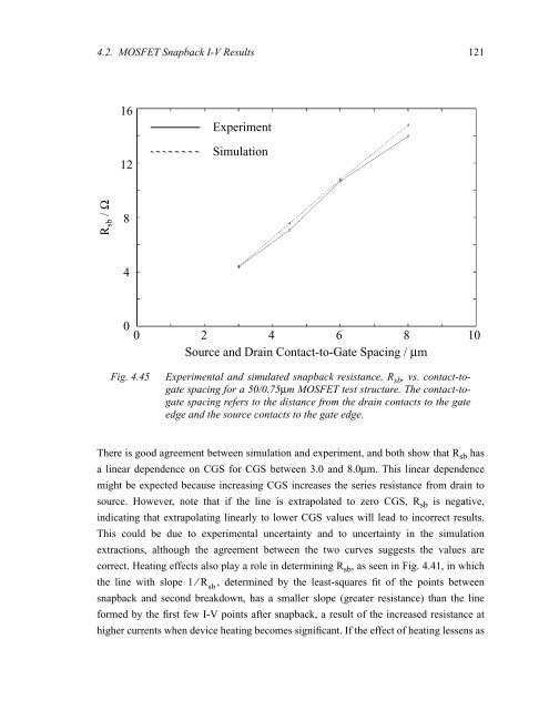
4.2. MOSFET Snapback I-V Results 121<br />
R sb / Ω<br />
16<br />
12<br />
8<br />
4<br />
Experiment<br />
Simulation<br />
0<br />
0 2 4 6 8 10<br />
Source <strong>and</strong> Drain Contact-to-Gate Spacing / µm<br />
Fig. 4.45 Experimental <strong>and</strong> simulated snapback resistance, R sb , vs. contact-togate<br />
spacing for a 50/0.75µm MOSFET test structure. The contact-togate<br />
spacing refers to the distance from the drain contacts to the gate<br />
edge <strong>and</strong> the source contacts to the gate edge.<br />
There is good agreement between simulation <strong>and</strong> experiment, <strong>and</strong> both show that Rsb has<br />
a linear dependence on CGS for CGS between 3.0 <strong>and</strong> 8.0µm. This linear dependence<br />
might be expected because increasing CGS increases the series resistance from drain to<br />
source. However, note that if the line is extrapolated to zero CGS, Rsb is negative,<br />
indicating that extrapolating linearly to lower CGS values will lead to incorrect results.<br />
This could be due to experimental uncertainty <strong>and</strong> to uncertainty in the simulation<br />
extractions, although the agreement between the two curves suggests the values are<br />
correct. Heating effects also play a role in determining Rsb , as seen in Fig. 4.41, in which<br />
the line with slope 1 ⁄<br />
Rsb, determined by the least-squares fit <strong>of</strong> the points between<br />
snapback <strong>and</strong> second breakdown, has a smaller slope (greater resistance) than the line<br />
formed by the first few I-V points after snapback, a result <strong>of</strong> the increased resistance at<br />
higher currents when device heating becomes significant. If the effect <strong>of</strong> heating lessens as


