

characterization, modeling, and design of esd protection circuits
characterization, modeling, and design of esd protection circuits
characterization, modeling, and design of esd protection circuits

Create successful ePaper yourself
Turn your PDF publications into a flip-book with our unique Google optimized e-Paper software.
40 Chapter 2. ESD Circuit Characterization <strong>and</strong> Design Issues<br />
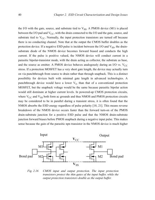
the I/O with the gate, source, <strong>and</strong> substrate tied to VSS . A PMOS device (M1) is placed<br />
between the I/O pad <strong>and</strong> VCC , with the drain connected to the I/O <strong>and</strong> the gate, source, <strong>and</strong><br />
substrate tied to VCC . Normally, the input <strong>protection</strong> transistors are turned <strong>of</strong>f because<br />
there is no conducting channel. Note that at the output the CMOS buffer doubles as the<br />
<strong>protection</strong> device. If a negative ESD pulse is incident between the I/O <strong>and</strong> VSS , the drainsubstrate<br />
diode <strong>of</strong> the NMOS device becomes forward biased <strong>and</strong> conducts the high<br />
current. If the pulse is positive valued, the NMOS device will conduct current in a<br />
parasitic bipolar-transistor mode, with the drain acting as collector, the substrate as base,<br />
<strong>and</strong> the source as emitter. A PMOS device behaves analogously during an I/O vs. VCC stress. If a <strong>protection</strong> MOSFET has a very short gate length, the device may actually turn<br />
on via punchthrough from source to drain rather than through snapback. This is a distinct<br />
possibility for devices built with minimal gate length in advanced technologies. A<br />
punchthrough device would have a lower Vt1 than that <strong>of</strong> a conventional <strong>protection</strong><br />
MOSFET, but the snapback voltage would be the same because parasitic bipolar action<br />
would still dominate at higher current levels. In powered-up CMOS <strong>protection</strong> <strong>circuits</strong>,<br />
where VCC <strong>and</strong> VSS both form ac grounds <strong>and</strong> thus NMOS <strong>and</strong> PMOS <strong>protection</strong> <strong>circuits</strong><br />
may be considered to be in parallel during a transient stress, it is <strong>of</strong>ten found that the<br />
NMOS absorbs the ESD energy regardless <strong>of</strong> pulse polarity [18, 21]. This means reverse<br />
breakdown <strong>of</strong> the NMOS device occurs faster than the forward turn-on <strong>of</strong> the PMOS<br />
drain-substrate junction for a positive ESD pulse <strong>and</strong> that the NMOS drain-substrate<br />
junction forward biases before PMOS snapback during a negative input pulse. This makes<br />
sense because the gain <strong>of</strong> the parasitic npn transistor in the NMOS device is much higher<br />
Input Output<br />
M1<br />
V CC<br />
Bond pad M2<br />
M2<br />
Bond pad<br />
V SS<br />
M1<br />
Fig. 2.16 CMOS input <strong>and</strong> output <strong>protection</strong>. The input <strong>protection</strong><br />
transistors protect the thin gates <strong>of</strong> the input buffer, while the<br />
output <strong>protection</strong> transistors double as the output buffer.


