

characterization, modeling, and design of esd protection circuits
characterization, modeling, and design of esd protection circuits
characterization, modeling, and design of esd protection circuits

Create successful ePaper yourself
Turn your PDF publications into a flip-book with our unique Google optimized e-Paper software.
26 Chapter 2. ESD Circuit Characterization <strong>and</strong> Design Issues<br />
log(I device / amps)<br />
V sb<br />
1/R sb<br />
V device / volts<br />
V t2 , I t2<br />
Second snapback<br />
V t1 , I t1<br />
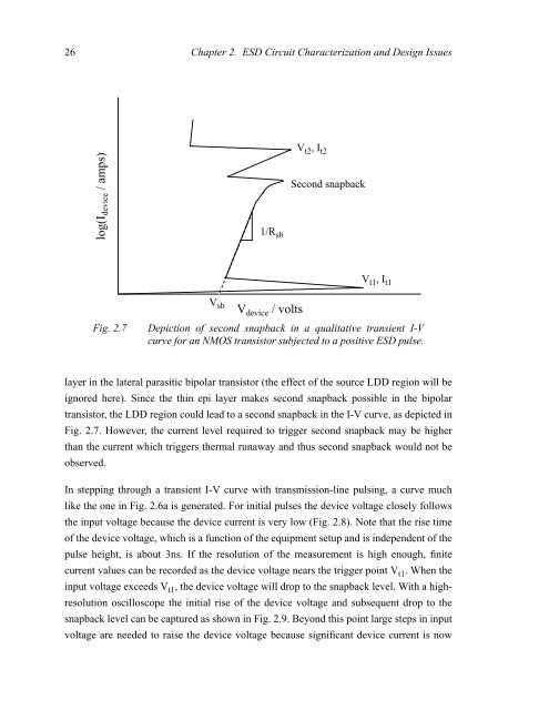
Fig. 2.7 Depiction <strong>of</strong> second snapback in a qualitative transient I-V<br />
curve for an NMOS transistor subjected to a positive ESD pulse.<br />
layer in the lateral parasitic bipolar transistor (the effect <strong>of</strong> the source LDD region will be<br />
ignored here). Since the thin epi layer makes second snapback possible in the bipolar<br />
transistor, the LDD region could lead to a second snapback in the I-V curve, as depicted in<br />
Fig. 2.7. However, the current level required to trigger second snapback may be higher<br />
than the current which triggers thermal runaway <strong>and</strong> thus second snapback would not be<br />
observed.<br />
In stepping through a transient I-V curve with transmission-line pulsing, a curve much<br />
like the one in Fig. 2.6a is generated. For initial pulses the device voltage closely follows<br />
the input voltage because the device current is very low (Fig. 2.8). Note that the rise time<br />
<strong>of</strong> the device voltage, which is a function <strong>of</strong> the equipment setup <strong>and</strong> is independent <strong>of</strong> the<br />
pulse height, is about 3ns. If the resolution <strong>of</strong> the measurement is high enough, finite<br />
current values can be recorded as the device voltage nears the trigger point Vt1 . When the<br />
input voltage exceeds Vt1 , the device voltage will drop to the snapback level. With a highresolution<br />
oscilloscope the initial rise <strong>of</strong> the device voltage <strong>and</strong> subsequent drop to the<br />
snapback level can be captured as shown in Fig. 2.9. Beyond this point large steps in input<br />
voltage are needed to raise the device voltage because significant device current is now


