Manual - 8500A Series Peak Power Meter - Giga-tronics
Manual - 8500A Series Peak Power Meter - Giga-tronics
Manual - 8500A Series Peak Power Meter - Giga-tronics
Create successful ePaper yourself
Turn your PDF publications into a flip-book with our unique Google optimized e-Paper software.
4<br />
Theory of Operation<br />
4.1 Introduction<br />
This chapter presents a functional description of the electrical assemblies in the Model 8501A and 8502A<br />
<strong>Peak</strong> <strong>Power</strong> <strong>Meter</strong>s (PPM). Table 8-1 in Chapter 8 lists the circuit assemblies by reference designation<br />
and includes the schematic diagram and assembly number for each board. Schematic diagrams and<br />
component layouts are in Chapter 8.<br />
The method to properly ground all PC boards is common throughout the PPM. Each PC board contains<br />
both input and output isolator stages to transfer the reference or ratio common ground when signals are<br />
passing between the PC boards to an on-board common ground. When any signals leave the boards, they<br />
pass through another isolator stage, which transfers them back to the between-the-boards reference<br />
ground.<br />
4.2 System Description<br />
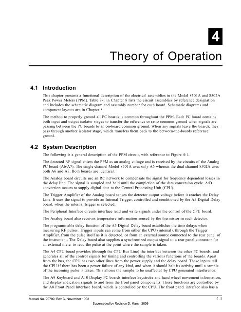
The following is a general description of the PPM circuit, with reference to Figure 4-1.<br />
The detected RF signal enters the PPM as an analog voltage and is received by the circuits of the Analog<br />
PC board (A6/A7). The single channel Model 8501A uses only A6 whereas the dual channel 8502A uses<br />
both A6 and A7. Both boards are identical.<br />
The Analog board circuits use an RC network to compensate the signal for frequency dependent losses in<br />
the delay line. The signal is sampled and held until the completion of the data conversion cycle. A/D<br />
conversion occurs to supply digital data to the Central Processing Unit (CPU).<br />
The Trigger Amplifier of the Analog board senses the detector output voltage before it reaches the Delay<br />
Line. It uses the signal to provide an Internal Trigger, controlled and conditioned by the A5 Digital Delay<br />
board, when the internal trigger is selected.<br />
The Peripheral Interface circuits interface read and write signals under the control of the CPU board.<br />
The Analog board also receives temperature information sensed by the thermistor in each detector.<br />
The programmable delay function of the A5 Digital Delay board establishes the time delays when<br />
measuring RF pulses. Trigger inputs can come from either the CPU (internal), through the Trigger<br />
Amplifier, from the pulse itself as it is detected, or from an external source connected to the rear panel of<br />
the instrument. The Delay board also supplies a synchronized output signal to a rear panel connector for<br />
an external meter to read the pulse at the point where the sample is taken.<br />
The A4 CPU board provides (through the CPU Bus Line) the interface between the other PC boards, and<br />
generates all of the control signals for timing and controlling the various functions of the boards. Apart<br />
from the bus, the CPU has two other lines from the power supply and the delay board. These inputs tell<br />
the CPU if there has been a power failure of any kind, and when it should halt its activity until a sample<br />
of the incoming pulse is taken. This allows the sample to be unaffected by CPU generated interference.<br />
The A9 Keyboard and A10 Display PC boards interface keystroke and hand wheel movement information,<br />
and display indication signals to and from the front panel components. These functions are controlled by<br />
the A8 Front Panel Interface board, which is controlled by the CPU. The front panel interface also has a<br />
<strong>Manual</strong> No. 20790, Rev C, November 1998 4-1<br />
Superceded by Revision D, March 2009


