Manual - 8500A Series Peak Power Meter - Giga-tronics
Manual - 8500A Series Peak Power Meter - Giga-tronics
Manual - 8500A Series Peak Power Meter - Giga-tronics
You also want an ePaper? Increase the reach of your titles
YUMPU automatically turns print PDFs into web optimized ePapers that Google loves.
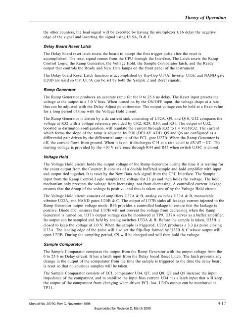
Theory of Operation<br />
the other counters, the load signal will be executed by having the multiplexer U16 delay the negative<br />
edge of the signal and inverting the signal using U15A, B & C.<br />
Delay Board Reset Latch<br />
The Delay board reset latch resets the board to accept the first trigger pulse after the reset is<br />
accomplished. The reset signal comes from the CPU through the Interface. The Latch resets the Ramp<br />
Control Logic, the Ramp Generator, the Voltage Hold, the Sample Comparator latch, and the Ready<br />
output that controls the Ready and New Data lamps on the front panel of the instrument.<br />
The Delay board Reset Latch function is accomplished by flip-flop U17A. Inverter U15E and NAND gate<br />
U20D are used so that U17A can be set by both the Sample 2 and Reset signals.<br />
Ramp Generator<br />
The Ramp Generator produces an accurate ramp for the 0 to 25.6 ns delay. The Reset input presets the<br />
voltage at the output to a 3.0 V bias. When turned on by the ON/OFF input, the voltage drops at a rate<br />
that can be adjusted with the Delay Adjust potentiometer. The output voltage can be held at a fixed value<br />
for a long period of time with the Voltage Hold circuit.<br />
The Ramp Generator is driven by a dc current sink consisting of U32A, Q9, and Q10. U32 compares the<br />
voltage at R32 with a voltage reference provided by CR2, R29, R30, and R31. The output of U32,<br />
boosted in darlington configuration, will regulate the current through R32 to I = Vref/R32. The current<br />
which forms the slope of the ramp is adjusted by R30 (DELAY ADJ). Q5 and Q6 are configured as a<br />
differential pair driven by the differential outputs of the ECL gate U27B. When the Ramp Generator is<br />
off, the current flows from ground. When it is on, it discharges C14 at a rate equal to dV/dT = I/C. The<br />
starting voltage is provided by the +10 V reference through R44 and R45 when switch U33C is closed.<br />
Voltage Hold<br />
The Voltage Hold circuit holds the output voltage of the Ramp Generator during the time it is waiting for<br />
the count output from the Counter. It consists of a double buffered sample and hold amplifier with input<br />
and output tied together. It is reset by the New Data Ack signal from the CPU Interface. The Sample<br />
input from the Ramp Control Logic samples the voltage for 33 µs and then holds the voltage. The hold<br />
mechanism only prevents the voltage from increasing, not from decreasing. A controlled current leakage<br />
ensures that the droop of the voltage is positive, and thus is taken care of by the Voltage Hold circuit.<br />
The Voltage Hold circuit consists of amplifiers U37A & B, analog switches U33A & B, monostable<br />
vibrator U22A, and NAND gates U20B & C. The output of U37B sinks all leakage current injected to the<br />
Ramp Generator output voltage mode. R46 provides a controlled leakage to ensure that the leakage is<br />
positive. Diode CR1 ensures that U37B will not prevent the voltage from decreasing when the Ramp<br />
Generator is turned on. U37’s output voltage can be monitored at TP9. U37A serves as a buffer amplifier.<br />
Its output can be sampled and held by analog switches U33A & B. Before the sample is taken, U33B is<br />
closed to keep the voltage at 3.0 V. When the sample is triggered, U22A produces a 3.3 µs pulse closing<br />
U33A. The leading edge of the pulse will also set the flip-flop formed by U22B & C whose output will<br />
open U33B. During the sampling period, C9 will be charged and will then hold the voltage.<br />
Sample Comparator<br />
The Sample Comparator compares the output from the Ramp Generator with the output voltage from the<br />
0 to 25.6 ns Delay circuit. It has a latch input from the Delay board Reset Latch. The latch prevents any<br />
change in the output of the comparator from the time the sample is triggered to the time the delay board<br />
is reset so that no spurious samples will be taken.<br />
The Sample Comparator consists of ECL comparator U34, Q7, and Q8. Q7 and Q8 increase the input<br />
impedance of the comparator, and to stabilize the input bias current. U34 has a latch input that will keep<br />
the output of the comparator from changing when driven ECL low. U34’s output can be monitored at<br />
TP11.<br />
<strong>Manual</strong> No. 20790, Rev C, November 1998 4-17<br />
Superceded by Revision D, March 2009


