Manual - 8500A Series Peak Power Meter - Giga-tronics
Manual - 8500A Series Peak Power Meter - Giga-tronics
Manual - 8500A Series Peak Power Meter - Giga-tronics
Create successful ePaper yourself
Turn your PDF publications into a flip-book with our unique Google optimized e-Paper software.
<strong>Series</strong> <strong>8500A</strong> <strong>Peak</strong> <strong>Power</strong> <strong>Meter</strong>s<br />
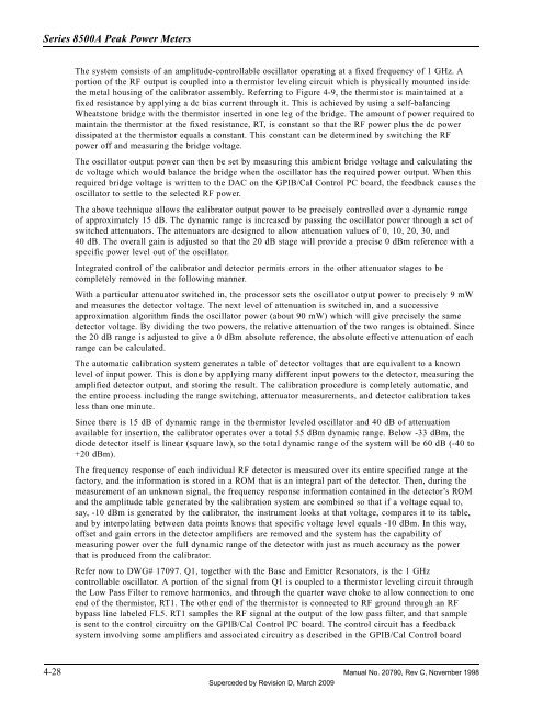
The system consists of an amplitude-controllable oscillator operating at a fixed frequency of 1 GHz. A<br />
portion of the RF output is coupled into a thermistor leveling circuit which is physically mounted inside<br />
the metal housing of the calibrator assembly. Referring to Figure 4-9, the thermistor is maintained at a<br />
fixed resistance by applying a dc bias current through it. This is achieved by using a self-balancing<br />
Wheatstone bridge with the thermistor inserted in one leg of the bridge. The amount of power required to<br />
maintain the thermistor at the fixed resistance, RT, is constant so that the RF power plus the dc power<br />
dissipated at the thermistor equals a constant. This constant can be determined by switching the RF<br />
power off and measuring the bridge voltage.<br />
The oscillator output power can then be set by measuring this ambient bridge voltage and calculating the<br />
dc voltage which would balance the bridge when the oscillator has the required power output. When this<br />
required bridge voltage is written to the DAC on the GPIB/Cal Control PC board, the feedback causes the<br />
oscillator to settle to the selected RF power.<br />
The above technique allows the calibrator output power to be precisely controlled over a dynamic range<br />
of approximately 15 dB. The dynamic range is increased by passing the oscillator power through a set of<br />
switched attenuators. The attenuators are designed to allow attenuation values of 0, 10, 20, 30, and<br />
40 dB. The overall gain is adjusted so that the 20 dB stage will provide a precise 0 dBm reference with a<br />
specific power level out of the oscillator.<br />
Integrated control of the calibrator and detector permits errors in the other attenuator stages to be<br />
completely removed in the following manner.<br />
With a particular attenuator switched in, the processor sets the oscillator output power to precisely 9 mW<br />
and measures the detector voltage. The next level of attenuation is switched in, and a successive<br />
approximation algorithm finds the oscillator power (about 90 mW) which will give precisely the same<br />
detector voltage. By dividing the two powers, the relative attenuation of the two ranges is obtained. Since<br />
the 20 dB range is adjusted to give a 0 dBm absolute reference, the absolute effective attenuation of each<br />
range can be calculated.<br />
The automatic calibration system generates a table of detector voltages that are equivalent to a known<br />
level of input power. This is done by applying many different input powers to the detector, measuring the<br />
amplified detector output, and storing the result. The calibration procedure is completely automatic, and<br />
the entire process including the range switching, attenuator measurements, and detector calibration takes<br />
less than one minute.<br />
Since there is 15 dB of dynamic range in the thermistor leveled oscillator and 40 dB of attenuation<br />
available for insertion, the calibrator operates over a total 55 dBm dynamic range. Below -33 dBm, the<br />
diode detector itself is linear (square law), so the total dynamic range of the system will be 60 dB (-40 to<br />
+20 dBm).<br />
The frequency response of each individual RF detector is measured over its entire specified range at the<br />
factory, and the information is stored in a ROM that is an integral part of the detector. Then, during the<br />
measurement of an unknown signal, the frequency response information contained in the detector’s ROM<br />
and the amplitude table generated by the calibration system are combined so that if a voltage equal to,<br />
say, -10 dBm is generated by the calibrator, the instrument looks at that voltage, compares it to its table,<br />
and by interpolating between data points knows that specific voltage level equals -10 dBm. In this way,<br />
offset and gain errors in the detector amplifiers are removed and the system has the capability of<br />
measuring power over the full dynamic range of the detector with just as much accuracy as the power<br />
that is produced from the calibrator.<br />
Refer now to DWG# 17097. Q1, together with the Base and Emitter Resonators, is the 1 GHz<br />
controllable oscillator. A portion of the signal from Q1 is coupled to a thermistor leveling circuit through<br />
the Low Pass Filter to remove harmonics, and through the quarter wave choke to allow connection to one<br />
end of the thermistor, RT1. The other end of the thermistor is connected to RF ground through an RF<br />
bypass line labeled FL5. RT1 samples the RF signal at the output of the low pass filter, and that sample<br />
is sent to the control circuitry on the GPIB/Cal Control PC board. The control circuit has a feedback<br />
system involving some amplifiers and associated circuitry as described in the GPIB/Cal Control board<br />
4-28 <strong>Manual</strong> No. 20790, Rev C, November 1998<br />
Superceded by Revision D, March 2009


