Manual - 8500A Series Peak Power Meter - Giga-tronics
Manual - 8500A Series Peak Power Meter - Giga-tronics
Manual - 8500A Series Peak Power Meter - Giga-tronics

Create successful ePaper yourself
Turn your PDF publications into a flip-book with our unique Google optimized e-Paper software.
<strong>Series</strong> <strong>8500A</strong> <strong>Peak</strong> <strong>Power</strong> <strong>Meter</strong>s<br />
inverse of what comes in through pin 16. The other half of U17B switches the signal into the oscillator<br />
control circuit which causes the oscillator to turn off. This is done when the switch is closed by causing<br />
the signal to unbalance the oscillator control circuit in such a way that no current can flow to the<br />
oscillator. Under that condition, C9 is disconnected from the circuit during the measuring period and the<br />
diode pair, CR1 and CR2, act to clamp the circuit to prevent U14’s output from going more than 1V from<br />
ground independent of the applied signal. U15 is a comparator that detects whether the output of U14,<br />
pin 6, is either positive or negative. The output of U15 then goes to the C port of U9 as an input. This<br />
tells the CPU whether U14’s output is either high or low as determined by the comparator. In the<br />
measurement mode, there is also a CPU driven successive approximation routine which puts a series of<br />
words out to the DAC, U10. Then, using standard successive approximation, the voltage level at TP9 is<br />
determined and placed in memory. On the basis of the voltage placed in memory and knowing the desired<br />
power out, the CPU can then calculate the voltage that must be written to U10 to control the oscillator<br />
for the desired output power. To briefly recap, the process is to measure the bridge voltage with no RF<br />
applied, determine the desired output power, and then write voltage corresponding to that power to the<br />
U10 DAC.<br />
When it is required that the oscillator be controlled, the B7 output of U9 will supply a high voltage<br />
signal to close the switch at C9 and open the switch on CR1 and CR2. C9 then serves to stabilize the<br />
complete control loop while the thermistor bridge system controls the oscillator. The control system<br />
operates in the following way. The oscillator provides RF power to the thermistor and, the more RF<br />
applied, the less dc power is required in the self-balancing bridge. Consequently, as the RF power<br />
increases the voltage at TP9 will decrease. This voltage feeds into the summing junction at U14. Since<br />
diodes CR1 and CR2 are switched out of the loop, the feedback circuit then goes from pin 6 of U14<br />
through R51 to the input of U18D. Pin 11 of U17B is open now, so there is no current fed to U18D from<br />
that point, and the voltage applied through R51 directly controls the current through Q6.<br />
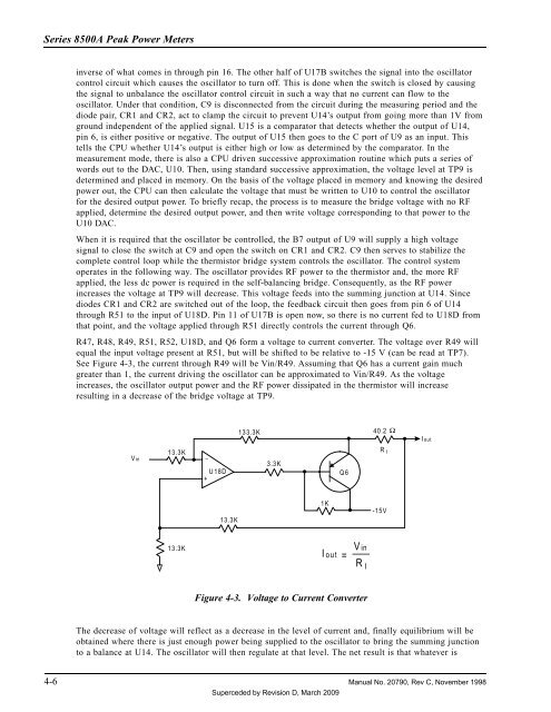
R47, R48, R49, R51, R52, U18D, and Q6 form a voltage to current converter. The voltage over R49 will<br />
equal the input voltage present at R51, but will be shifted to be relative to -15 V (can be read at TP7).<br />
See Figure 4-3, the current through R49 will be Vin/R49. Assuming that Q6 has a current gain much<br />
greater than 1, the current driving the oscillator can be approximated to Vin/R49. As the voltage<br />
increases, the oscillator output power and the RF power dissipated in the thermistor will increase<br />
resulting in a decrease of the bridge voltage at TP9.<br />
133.3K<br />
40.2 Ω<br />
I out<br />
V in<br />
13.3K<br />
_<br />
U18D<br />
+<br />
3.3K<br />
Q6<br />
R I<br />
13.3K<br />
1K<br />
-15V<br />
13.3K<br />
I out<br />
= V in<br />
R I<br />
Figure 4-3. Voltage to Current Converter<br />
The decrease of voltage will reflect as a decrease in the level of current and, finally equilibrium will be<br />
obtained where there is just enough power being supplied to the oscillator to bring the summing junction<br />
to a balance at U14. The oscillator will then regulate at that level. The net result is that whatever is<br />
4-6 <strong>Manual</strong> No. 20790, Rev C, November 1998<br />
Superceded by Revision D, March 2009