- Page 1 and 2:
Manual Part Number: 20790 Revision
- Page 3 and 4:
Errata Sheet for Series 8500A Peak
- Page 5 and 6:
QUICK REFERENCE CARD Giga-tronics M
- Page 7 and 8:
Series 8500A Peak Power Meters 2.8.
- Page 9 and 10:
Series 8500A Peak Power Meters 6
- Page 11 and 12:
Series 8500A Peak Power Meters E
- Page 13 and 14:
Series 8500A Peak Power Meters List
- Page 15 and 16:
Series 8500A Peak Power Meters x Ma
- Page 17 and 18:
Series 8500A Peak Power Meters Symb
- Page 19 and 20:
Series 8500A Peak Power Meters xiv
- Page 21 and 22:
Series 8500A Peak Power Meters xvi
- Page 23 and 24:
Series 8500A Peak Power Meters 1.1.
- Page 25 and 26:
Series 8500A Peak Power Meters 1.2
- Page 27 and 28:
Series 8500A Peak Power Meters Auxi
- Page 29 and 30:
Series 8500A Peak Power Meters 1.3
- Page 31 and 32:
Series 8500A Peak Power Meters ☛
- Page 33 and 34:
Series 8500A Peak Power Meters 2.2.
- Page 35 and 36:
Series 8500A Peak Power Meters 4 De
- Page 37 and 38:
Series 8500A Peak Power Meters 7 Cl
- Page 39 and 40:
Series 8500A Peak Power Meters 2.5
- Page 41 and 42:
Series 8500A Peak Power Meters Inte
- Page 43 and 44:
Series 8500A Peak Power Meters 2.7
- Page 45 and 46:
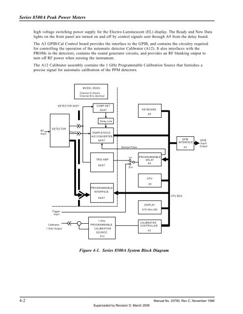
Series 8500A Peak Power Meters 2.8
- Page 47 and 48:
Series 8500A Peak Power Meters In t
- Page 49 and 50:
Series 8500A Peak Power Meters Wait
- Page 51 and 52:
Series 8500A Peak Power Meters time
- Page 53 and 54:
Series 8500A Peak Power Meters 2.8.
- Page 55 and 56:
Series 8500A Peak Power Meters 2.8.
- Page 57 and 58:
Series 8500A Peak Power Meters 2.8.
- Page 59 and 60:
Series 8500A Peak Power Meters 2.9
- Page 61 and 62:
Series 8500A Peak Power Meters 2.10
- Page 63 and 64:
Series 8500A Peak Power Meters 1. C
- Page 65 and 66:
Series 8500A Peak Power Meters 3. V
- Page 67 and 68:
Series 8500A Peak Power Meters Figu
- Page 69 and 70:
Series 8500A Peak Power Meters 2.13
- Page 71 and 72:
Series 8500A Peak Power Meters 2.14
- Page 73 and 74:
Series 8500A Peak Power Meters 2.15
- Page 75 and 76:
Series 8500A Peak Power Meters ☛
- Page 77 and 78:
Series 8500A Peak Power Meters 2-48
- Page 79 and 80: Series 8500A Peak Power Meters 3.2
- Page 81 and 82: Series 8500A Peak Power Meters 3.2.
- Page 83 and 84: Series 8500A Peak Power Meters The
- Page 85 and 86: Series 8500A Peak Power Meters Plot
- Page 87 and 88: Series 8500A Peak Power Meters Temp
- Page 89 and 90: Series 8500A Peak Power Meters 3.2.
- Page 91 and 92: Series 8500A Peak Power Meters 3.3
- Page 93 and 94: Series 8500A Peak Power Meters Outp
- Page 95 and 96: Series 8500A Peak Power Meters Dete
- Page 97 and 98: Series 8500A Peak Power Meters User
- Page 99 and 100: Series 8500A Peak Power Meters Rela
- Page 101 and 102: Series 8500A Peak Power Meters 3.3.
- Page 103 and 104: Series 8500A Peak Power Meters Auto
- Page 105 and 106: Series 8500A Peak Power Meters Auto
- Page 107 and 108: Series 8500A Peak Power Meters MRKA
- Page 109 and 110: Series 8500A Peak Power Meters (n =
- Page 111 and 112: Series 8500A Peak Power Meters 3.3.
- Page 113 and 114: Series 8500A Peak Power Meters 3.4
- Page 115 and 116: Series 8500A Peak Power Meters 3.5
- Page 117 and 118: Series 8500A Peak Power Meters Over
- Page 119 and 120: Series 8500A Peak Power Meters Deci
- Page 121 and 122: Series 8500A Peak Power Meters 3.8
- Page 123 and 124: Series 8500A Peak Power Meters Comm
- Page 125 and 126: Series 8500A Peak Power Meters Comm
- Page 127 and 128: Series 8500A Peak Power Meters Comm
- Page 129: Series 8500A Peak Power Meters 3.9
- Page 133 and 134: Series 8500A Peak Power Meters 4.2.
- Page 135 and 136: Series 8500A Peak Power Meters inve
- Page 137 and 138: Series 8500A Peak Power Meters 4.2.
- Page 139 and 140: Series 8500A Peak Power Meters Addr
- Page 141 and 142: Series 8500A Peak Power Meters 4.2.
- Page 143 and 144: Series 8500A Peak Power Meters Figu
- Page 145 and 146: Series 8500A Peak Power Meters Trig
- Page 147 and 148: Series 8500A Peak Power Meters Ramp
- Page 149 and 150: Series 8500A Peak Power Meters 4.2.
- Page 151 and 152: Series 8500A Peak Power Meters feed
- Page 153 and 154: Series 8500A Peak Power Meters 4.2.
- Page 155 and 156: Series 8500A Peak Power Meters A8 T
- Page 157 and 158: Series 8500A Peak Power Meters The
- Page 159 and 160: Series 8500A Peak Power Meters 4-30
- Page 161 and 162: Series 8500A Peak Power Meters 5.2
- Page 163 and 164: Series 8500A Peak Power Meters 5.2.
- Page 165 and 166: Series 8500A Peak Power Meters 5.2.
- Page 167 and 168: Series 8500A Peak Power Meters 5.3
- Page 169 and 170: Series 8500A Peak Power Meters 5.3.
- Page 171 and 172: Series 8500A Peak Power Meters 5.3.
- Page 173 and 174: Series 8500A Peak Power Meters 7. P
- Page 175 and 176: Series 8500A Peak Power Meters 5.3.
- Page 177 and 178: Series 8500A Peak Power Meters Tabl
- Page 179 and 180: Series 8500A Peak Power Meters 4. P
- Page 181 and 182:
Peak Power Linearity Data Step Atte
- Page 183 and 184:
Series 8500A Peak Power Meters 5-24
- Page 185 and 186:
Series 8500A Peak Power Meters 6.2.
- Page 187 and 188:
Series 8500A Peak Power Meters b. P
- Page 189 and 190:
Series 8500A Peak Power Meters Self
- Page 191 and 192:
Series 8500A Peak Power Meters 8502
- Page 193 and 194:
Series 8500A Peak Power Meters 2051
- Page 195 and 196:
Series 8500A Peak Power Meters 2114
- Page 197 and 198:
Series 8500A Peak Power Meters 1693
- Page 199 and 200:
Series 8500A Peak Power Meters 1699
- Page 201 and 202:
Series 8500A Peak Power Meters 1699
- Page 203 and 204:
Series 8500A Peak Power Meters 2101
- Page 205 and 206:
Series 8500A Peak Power Meters 1687
- Page 207 and 208:
Series 8500A Peak Power Meters 1687
- Page 209 and 210:
Series 8500A Peak Power Meters 1668
- Page 211 and 212:
Series 8500A Peak Power Meters 1668
- Page 213 and 214:
Series 8500A Peak Power Meters 2074
- Page 215 and 216:
Series 8500A Peak Power Meters 2074
- Page 217 and 218:
Series 8500A Peak Power Meters 2074
- Page 219 and 220:
Series 8500A Peak Power Meters 2019
- Page 221 and 222:
Series 8500A Peak Power Meters 2019
- Page 223 and 224:
Series 8500A Peak Power Meters 2005
- Page 225 and 226:
Series 8500A Peak Power Meters 7.3
- Page 227 and 228:
Series 8500A Peak Power Meters CAGE
- Page 229 and 230:
Series 8500A Peak Power Meters CAGE
- Page 231 and 232:
Series 8500A Peak Power Meters CAGE
- Page 233:
Series 8500A Peak Power Meters 8-2
- Page 267 and 268:
Series 8500A Peak Power Meters Func
- Page 269 and 270:
Series 8500A Peak Power Meters Chan
- Page 271 and 272:
Series 8500A Peak Power Meters A-6
- Page 273 and 274:
Series 8500A Peak Power Meters MENU
- Page 275 and 276:
Series 8500A Peak Power Meters B.3
- Page 277 and 278:
Series 8500A Peak Power Meters MODE
- Page 279 and 280:
Series 8500A Peak Power Meters D.2
- Page 281 and 282:
Series 8500A Peak Power Meters D.3
- Page 283 and 284:
Series 8500A Peak Power Meters D.3.
- Page 285 and 286:
Series 8500A Peak Power Meters D.5.
- Page 287 and 288:
Series 8500A Peak Power Meters Figu
- Page 289 and 290:
Series 8500A Peak Power Meters E.3
- Page 291 and 292:
Series 8500A Peak Power Meters SRQ
- Page 293 and 294:
Series 8500A Peak Power Meters Trou
- Page 295 and 296:
Series 8500A Peak Power Meters Summ
- Page 297:
Series 8500A Peak Power Meters Inde