Manual - 8500A Series Peak Power Meter - Giga-tronics
Manual - 8500A Series Peak Power Meter - Giga-tronics
Manual - 8500A Series Peak Power Meter - Giga-tronics

Create successful ePaper yourself
Turn your PDF publications into a flip-book with our unique Google optimized e-Paper software.
<strong>Series</strong> <strong>8500A</strong> <strong>Peak</strong> <strong>Power</strong> <strong>Meter</strong>s<br />
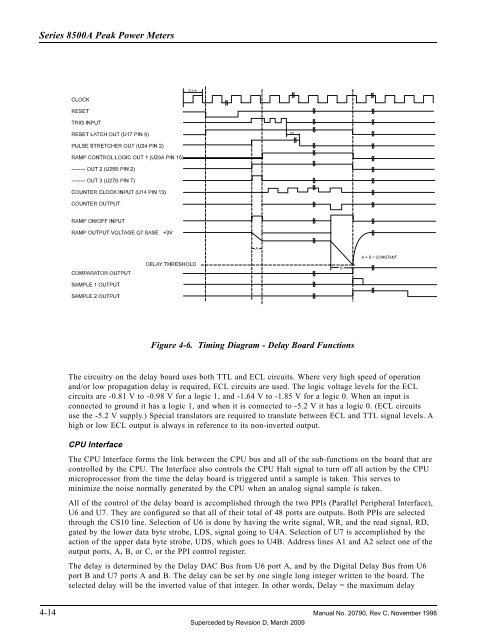
Figure 4-6. Timing Diagram - Delay Board Functions<br />
The circuitry on the delay board uses both TTL and ECL circuits. Where very high speed of operation<br />
and/or low propagation delay is required, ECL circuits are used. The logic voltage levels for the ECL<br />
circuits are -0.81 V to -0.98 V for a logic 1, and -1.64 V to -1.85 V for a logic 0. When an input is<br />
connected to ground it has a logic 1, and when it is connected to -5.2 V it has a logic 0. (ECL circuits<br />
use the -5.2 V supply.) Special translators are required to translate between ECL and TTL signal levels. A<br />
high or low ECL output is always in reference to its non-inverted output.<br />
CPU Interface<br />
The CPU Interface forms the link between the CPU bus and all of the sub-functions on the board that are<br />
controlled by the CPU. The Interface also controls the CPU Halt signal to turn off all action by the CPU<br />
microprocessor from the time the delay board is triggered until a sample is taken. This serves to<br />
minimize the noise normally generated by the CPU when an analog signal sample is taken.<br />
All of the control of the delay board is accomplished through the two PPIs (Parallel Peripheral Interface),<br />
U6 and U7. They are configured so that all of their total of 48 ports are outputs. Both PPIs are selected<br />
through the CS10 line. Selection of U6 is done by having the write signal, WR, and the read signal, RD,<br />
gated by the lower data byte strobe, LDS, signal going to U4A. Selection of U7 is accomplished by the<br />
action of the upper data byte strobe, UDS, which goes to U4B. Address lines A1 and A2 select one of the<br />
output ports, A, B, or C, or the PPI control register.<br />
The delay is determined by the Delay DAC Bus from U6 port A, and by the Digital Delay Bus from U6<br />
port B and U7 ports A and B. The delay can be set by one single long integer written to the board. The<br />
selected delay will be the inverted value of that integer. In other words, Delay = the maximum delay<br />
4-14 <strong>Manual</strong> No. 20790, Rev C, November 1998<br />
Superceded by Revision D, March 2009