- Page 1 and 2:
Constraints Guide UG625 (v. 13.2) J
- Page 3 and 4: Table of Contents Revision History
- Page 5 and 6: IBUF_DELAY_VALUE (Input Buffer Dela
- Page 7 and 8: Constraint Types Attributes and Con
- Page 9 and 10: Grouping Constraints for Timing Cha
- Page 11 and 12: The name qualifier can include the
- Page 13 and 14: Physical Constraints Mapping Note T
- Page 15 and 16: Placement Constraints Chapter 1: Co
- Page 17 and 18: Routing Directives Routing directiv
- Page 19 and 20: Timing Constraints Chapter 1: Const
- Page 21 and 22: UCF Timing Constraint Support From-
- Page 23 and 24: Timing Model Constraint Priority Ch
- Page 25 and 26: Chapter 2 Entry Strategies for Xili
- Page 27 and 28: Constraint Schematic VHDL Verilog L
- Page 29 and 30: An attribute can be declared in an
- Page 31 and 32: User Constraints File (UCF) UCF Flo
- Page 33 and 34: Syntax Chapter 2: Entry Strategies
- Page 35 and 36: Entering Multiple Constraints File
- Page 37 and 38: Chapter 2: Entry Strategies for Xil
- Page 39 and 40: Running Constraints Editor As a Sta
- Page 41 and 42: Defining I/O Pin Configurations Cha
- Page 43 and 44: Placement LOC Constraint Assignment
- Page 45 and 46: Verilog Example -------------module
- Page 47 and 48: Chapter 2: Entry Strategies for Xil
- Page 49 and 50: Timing Specification Priorities Cha
- Page 51 and 52: Timing Constraint Strategies Chapte
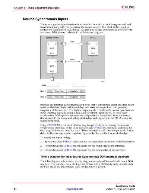
- Page 53: Chapter 3: Timing Constraint Strate
- Page 57 and 58: The PERIOD constraint syntax for th
- Page 59 and 60: Example Chapter 3: Timing Constrain
- Page 61 and 62: Chapter 3: Timing Constraint Strate
- Page 63 and 64: The global OFFSET OUT constraints f
- Page 65 and 66: Multi-Cycle Paths Chapter 3: Timing
- Page 67 and 68: Xilinx Constraints Each Xilinx® co
- Page 69 and 70: RANGE Chapter 4: Xilinx Constraints
- Page 71 and 72: Chapter 4: Xilinx Constraints Range
- Page 73 and 74: COMPRESSION GROUP PLACE Chapter 4:
- Page 75 and 76: Defining From Timing Groups Chapter
- Page 77 and 78: BEL (BEL) The BEL (BEL) constraint:
- Page 79 and 80: BLKNM (Block Name) Architecture Sup
- Page 81 and 82: BUFG (BUFG) The BUFG (BUFG) constra
- Page 83 and 84: Clock Dedicated Route (CLOCK_DEDICA
- Page 85 and 86: COMPGRP (Component Group) Architect
- Page 87 and 88: • S_SELECTMAP16 Slave SelectMAP M
- Page 89 and 90: Verilog Syntax Chapter 4: Xilinx Co
- Page 91 and 92: Verilog Syntax Chapter 4: Xilinx Co
- Page 93 and 94: PCF Syntax CONFIG DCI_CASCADE = ",
- Page 95 and 96: Default (DEFAULT) Chapter 4: Xilinx
- Page 97 and 98: Example (* KEEPER = “TRUE” *) D
- Page 99 and 100: DIFF_TERM (Diff_Term) Architecture
- Page 101 and 102: DIRECTED_ROUTING (Directed Routing)
- Page 103 and 104: DISABLE (Disable) The DISABLE (Disa
- Page 105 and 106:
DRIVE (Drive) The DRIVE (Drive) con
- Page 107 and 108:
XCF Syntax MODEL “entity_name”
- Page 109 and 110:
ENABLE (Enable) The ENABLE (Enable)
- Page 111 and 112:
ENABLE_SUSPEND (Enable Suspend) Arc
- Page 113 and 114:
Verilog Syntax Chapter 4: Xilinx Co
- Page 115 and 116:
Constraints Editor Syntax Chapter 4
- Page 117 and 118:
VHDL Syntax Declare the VHDL constr
- Page 119 and 120:
UCF and NCF Syntax NET “signal_na
- Page 121 and 122:
Chapter 4: Xilinx Constraints You a
- Page 123 and 124:
Constraints Editor Syntax Chapter 4
- Page 125 and 126:
HBLKNM (Hierarchical Block Name) Ar
- Page 127 and 128:
HIODELAY_GROUP (HIODELAY Group) Arc
- Page 129 and 130:
VHDL Syntax Declare the VHDL constr
- Page 131 and 132:
HU_SET (HU Set) The HU_SET (HU Set)
- Page 133 and 134:
IBUF_DELAY_VALUE (Input Buffer Dela
- Page 135 and 136:
IFD_DELAY_VALUE (IFD Delay Value) T
- Page 137 and 138:
IN_TERM (In Term) Architecture Supp
- Page 139 and 140:
INREG (Input Registers) Architectur
- Page 141 and 142:
IOB (IOB) The IOB constraint: • I
- Page 143 and 144:
IOBDELAY (Input Output Block Delay)
- Page 145 and 146:
IODELAY_GROUP (IODELAY Group) Limit
- Page 147 and 148:
IOSTANDARD (Input Output Standard)
- Page 149 and 150:
Pinout and Area Constraints Editor
- Page 151 and 152:
Verilog Syntax Chapter 4: Xilinx Co
- Page 153 and 154:
Architecture Support Applicable Ele
- Page 155 and 156:
Keeper (KEEPER) Architecture Suppor
- Page 157 and 158:
LOC (Location) The LOC (Location) c
- Page 159 and 160:
Chapter 4: Xilinx Constraints The w
- Page 161 and 162:
LOC Range Constraint Examples Const
- Page 163 and 164:
PlanAhead Syntax Chapter 4: Xilinx
- Page 165 and 166:
Schematic LOC=P17 Chapter 4: Xilinx
- Page 167 and 168:
Example One Chapter 4: Xilinx Const
- Page 169 and 170:
Slices Prohibited Example Two Chapt
- Page 171 and 172:
LOCK_PINS (Lock Pins) Architecture
- Page 173 and 174:
where value is any chosen name unde
- Page 175 and 176:
MAP (Map) Architecture Support Appl
- Page 177 and 178:
Specify the Verilog constraint as f
- Page 179 and 180:
Architecture Support Applicable Ele
- Page 181 and 182:
MAXDELAY (Maximum Delay) Architectu
- Page 183 and 184:
PCF Syntax item MAXDELAY = maxvalue
- Page 185 and 186:
MAXSKEW (Maximum Skew) The MAXSKEW
- Page 187 and 188:
FPGA Editor Syntax Chapter 4: Xilin
- Page 189 and 190:
MIODELAY_GROUP (MIODELAY Group) Arc
- Page 191 and 192:
VHDL Syntax Declare the VHDL constr
- Page 193 and 194:
UCF and NCF Syntax Chapter 4: Xilin
- Page 195 and 196:
where Chapter 4: Xilinx Constraints
- Page 197 and 198:
Falling Edge Constraints Chapter 4:
- Page 199 and 200:
PlanAhead Syntax Chapter 4: Xilinx
- Page 201 and 202:
where Chapter 4: Xilinx Constraints
- Page 203 and 204:
UCF Syntax NET “clock” TNM_NET
- Page 205 and 206:
Verilog Syntax Chapter 4: Xilinx Co
- Page 207 and 208:
Attribute OUT_TERM: string; Specify
- Page 209 and 210:
TIMESPEC PERIOD Method Chapter 4: X
- Page 211 and 212:
Examples of a Primary Clock with De
- Page 213 and 214:
where • period is the required cl
- Page 215 and 216:
New PERIOD Specifications Output Pi
- Page 217 and 218:
Post CRC (POST_CRC) Architecture Su
- Page 219 and 220:
Post CRC Frequency (POST_CRC_FREQ)
- Page 221 and 222:
Post CRC Signal (POST_CRC_SIGNAL) A
- Page 223 and 224:
PRIORITY (Priority) Architecture Su
- Page 225 and 226:
The following are not supported: Ch
- Page 227 and 228:
PULLDOWN (Pulldown) Architecture Su
- Page 229 and 230:
PULLUP (Pullup) Architecture Suppor
- Page 231 and 232:
PWR_MODE (Power Mode) Architecture
- Page 233 and 234:
REG (Registers) The REG (Registers)
- Page 235 and 236:
RLOC (Relative Location) The Relati
- Page 237 and 238:
RLOC = X3Y4 Chapter 4: Xilinx Const
- Page 239 and 240:
Linking Sets Set Linkage Chapter 4:
- Page 241 and 242:
Chapter 4: Xilinx Constraints by th
- Page 243 and 244:
Linking Two HU_SET Sets Chapter 4:
- Page 245 and 246:
Specify the VHDL constraint as foll
- Page 247 and 248:
Chapter 4: Xilinx Constraints Diffe
- Page 249 and 250:
H_SET (H Set) Chapter 4: Xilinx Con
- Page 251 and 252:
Chapter 4: Xilinx Constraints The n
- Page 253 and 254:
Syntax Examples Chapter 4: Xilinx C
- Page 255 and 256:
RLOC_RANGE (Relative Location Range
- Page 257 and 258:
where the relative X values (m1 and
- Page 259 and 260:
VHDL Syntax Declare the VHDL constr
- Page 261 and 262:
UCF and NCF Syntax NET “mysignal
- Page 263 and 264:
Verilog Syntax Chapter 4: Xilinx Co
- Page 265 and 266:
VHDL Syntax Chapter 4: Xilinx Const
- Page 267 and 268:
SLOW (Slow) The SLOW (Slow) constra
- Page 269 and 270:
STEPPING (Stepping) Architecture Su
- Page 271 and 272:
VHDL Syntax Chapter 4: Xilinx Const
- Page 273 and 274:
Verilog Syntax Chapter 4: Xilinx Co
- Page 275 and 276:
Constraints Editor Syntax Chapter 4
- Page 277 and 278:
Chapter 4: Xilinx Constraints The f
- Page 279 and 280:
TIMEGRP (Timing Group) The TIMEGRP
- Page 281 and 282:
Defining Latch Subgroups by Gate Se
- Page 283 and 284:
Chapter 4: Xilinx Constraints When
- Page 285 and 286:
PCF Syntax TIMEGRP name; TIMEGRP na
- Page 287 and 288:
Separators FROM-TO Syntax TIMESPEC
- Page 289 and 290:
TNM (Timing Name) Chapter 4: Xilinx
- Page 291 and 292:
Chapter 4: Xilinx Constraints A qua
- Page 293 and 294:
TNM_NET (Timing Name Net) The TNM_N
- Page 295 and 296:
Schematic Syntax • Attach to a ne
- Page 297 and 298:
TPSYNC (Timing Point Synchronizatio
- Page 299 and 300:
UCF and NCF Syntax NET “net_name
- Page 301 and 302:
Using TPTHRU in a FROM TO Constrain
- Page 303 and 304:
TSidentifier (Timing Specification
- Page 305 and 306:
Ignoring Paths Note This form is no
- Page 307 and 308:
VHDL Syntax Declare the VHDL constr
- Page 309 and 310:
UCF and NCF Syntax Chapter 4: Xilin
- Page 311 and 312:
Verilog Syntax Chapter 4: Xilinx Co
- Page 313 and 314:
Chapter 4: Xilinx Constraints If yo
- Page 315 and 316:
Use Low Skew Lines (USELOWSKEWLINES
- Page 317 and 318:
VCCAUX (VCCAUX) Architecture Suppor
- Page 319 and 320:
UCF and NCF Syntax Chapter 4: Xilin
- Page 321 and 322:
VREF (VREF) The VREF (VREF) constra
- Page 323 and 324:
XBLKNM (XBLKNM) Architecture Suppor
- Page 325:
Additional Resources Appendix • X


