Suprem III - Stanford Technology CAD Home Page
Suprem III - Stanford Technology CAD Home Page
Suprem III - Stanford Technology CAD Home Page
Create successful ePaper yourself
Turn your PDF publications into a flip-book with our unique Google optimized e-Paper software.
-114-<br />
<strong>Suprem</strong>-<strong>III</strong> User´s Manual<br />
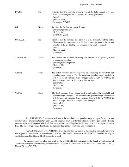
PTYPE log Specifies that the majority impurity type at the bulk contact is p-type.<br />
Used only in conjunction with the BULKCONC parameter.<br />
(unit: )<br />
(default: false.)<br />
(synonym: P-TYPE)<br />
Q.F Num Specifies the fixed oxide charge density.<br />
(unit: charges/unit area)<br />
(default: 0.0)<br />
(synonym: Q.SS)<br />
SURFACE log Specifies that the substrate bias contact is at the top surface of the wafer.<br />
This causes the concentration at the first or topmost point in the current<br />
structure to be used as the concentration at the point of contact.<br />
(unit: )<br />
(default: true)<br />
(synonym: )<br />
TEMPERAT Num The calculations are done assuming that the device is operating at the<br />
temperature specified.<br />
(unit: degrees centigrade)<br />
(default: 27.0)<br />
(synonym: )<br />
V.SUB1 Num The initial substrate bias voltage used in calculating the threshold and<br />
punchthrough voltages. The threshold and punchthrough calculations<br />
will be done at substrate bias voltages from V.SUB1 to V.SUB2 in<br />
DV.SUB steps. At most 20 steps will be attempted.<br />
(unit: volts)<br />
(default: 0.0)<br />
(synonym: )<br />
V.SUB2 Num The final substrate bias voltage used in calculating the threshold and<br />
punchthrough voltages. The threshold and punchthrough calculations<br />
will be done at substrate bias voltages from V.SUB1 to V.SUB2 in<br />
DV.SUB steps. At most 20 steps will be attempted.<br />
(unit: volts)<br />
(default: 5.0)<br />
(synonym: )<br />
The V.THRESHOLD statement calculates the threshold and punchthrough voltages for the current<br />
structure at one or more substrate biases. A MIS structure must exist for the calculations to be performed. If more<br />
than one substrate bias point is desired, then the first and last and optionally the increment bias voltages are specified.<br />
The oxide fixed charge density and the substrate bias contact point may also be specified.<br />
Normally the results of the V.THRESHOLD calculations are output to the standard output, however if a<br />
file is specified, the results are instead sent to that file. The results of several V.THRESHOLD calculations may be<br />
sent to the same file if the APPEND parameter is used.<br />
An explanation of the algorithm used by the V.THRESHOLD statement can be found in ‘Calculation of<br />
Threshold Voltage in Nonuniformly Doped MOSFETS’, by D. A. Antoniadis, IEEE Trans. E. D., Vol. ED-31, No. 3,<br />
March 1984, pp 303-307.


